The implementation of diamond wire wafer cutting dramatically reduced kerf – the crystalline material that is wasted when a solar ingot is sliced into wafers. Now epitaxy allows kerf losses to be kicked to the curb and Germany’s NexWafe is taking its epitaxial wafer production to commercial scale. Chief executive officer (CEO)Davor Sutija spoke with pv magazine shortly after the ground-breaking ceremony at its new facility in October.
Sutija says that wafers with a thickness of 90 microns can be produced with high yield with the NexWafe epitaxial process.
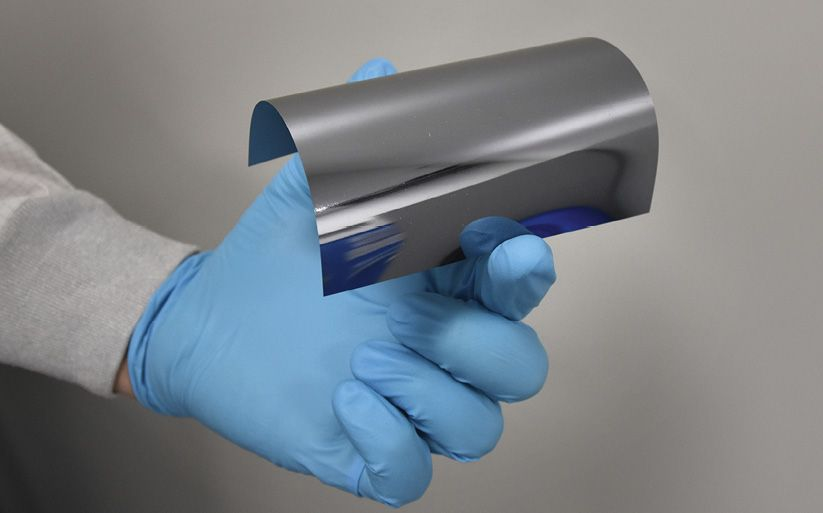
Image: Nexwafe
Stay informed
pv magazine is the leading trade media platform covering the global solar photovoltaics industry. Log in or purchase a digital or print version of this issue to read this article in full.
The cookie settings on this website are set to "allow cookies" to give you the best browsing experience possible. If you continue to use this website without changing your cookie settings or you click "Accept" below then you are consenting to this.