Finnish researchers at Aalto University investigated using a one-step femtosecond laser direct writing process to produce a proof-of-concept based on nanostructured commercially available borosilicate glass for building-integrated photovoltaics (BIPV) applications.
It is seen as an alternative to conventional luminescent solar concentrators (LSC). In the past, LSC technology has been proposed to improve PV panel efficiency or to enhance plant growth in greenhouses, and in other industries such as photonic devices in photo microreactors for fine chemical production.
“The key novelty of our research lies in applying a nanopattern to window glass using a very simple, cost-effective, single-step laser process,” Xiaolong Liu, corresponding author told pv magazine, pointing out that, unlike LSC devices, which rely on depositing luminescent materials on glass, the method directly modifies the glass surface itself.
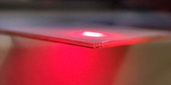
“This pattern alters the way light propagates through the glass, whereas in a conventional window, nearly all light passes straight through, and in an LSC light is absorbed and re-emitted by luminescent materials, our patterned surface allows us to tailor the light path, guiding up to 10% of it to propagate along the glass toward its edge,” he also said.
“This controlled redirection opens up exciting possibilities for building-integrated photovoltaics (BIPV), where the guided light can be harvested at the window frame. Moreover, the simplicity of the fabrication process provides potential for greater design flexibility for complex aesthetic patterns,” Liu added. “Our next steps focus on improving the optical efficiency of the nanostructured glass, which is still relatively low at 0.66% and needs further enhancement.”
Indeed, the calculated optical efficiency was estimated to be 0.66 % for the 400 mm/s sample, which the researchers contrasted with LSC designs in the literature that achieved an optical power efficiency of 7.8%.
The details of the research work appear in “Femtosecond-laser-surface-nanostructured glass for building-integrated photovoltaics,” published by Materials & Design.
The team used commercially available glass wafers with a thickness of 0.7 mm as the substrate. The laser texturing was a maskless process in ambient air using an off-the-shelf femtosecond laser, operating at a working range of 520 nm, delivering a pulse duration of 324 fs, a repetition rate of 417 kHz, and an approximate spot diameter of 10 µm at the focal point, according to the research.
The laser spot was focused by lenses that had focal lengths of 100 mm and a working range of 515-540 nm. The samples were scanned line by line with linear polarization direction aligned to the scanning direction. The line scan had a spacing of 10 µm aligning with the spot diameter to ensure the whole surface was patterned by the laser.
“The fluence was kept constant at 34.4 J/cm2, and the scan speed was adjusted within a range of 200–2000 mm/s,” said the team.
Examining the results, it said that the nanostructured glass, particularly when processed at an optimal speed of 400 mm/s, “significantly” enhanced the waveguiding capability and overall optical efficiency of the concentrator system.
A photocurrent increase of up to 55-fold compared to unprocessed glass was measured. “We attribute this to the balance between total scattering ability and transmittance; lower scan speeds produce more nanoparticles that efficiently scatter light but also inhibit light transmission through the glass,” said the researchers.
Characterizing the effect was challenging, according to Liu who said that measuring how much light was scattered to the edges in a reliable way was “not trivial,” as conventional optical measurements are typically designed for transmission and reflection rather than lateral light propagation. “Developing an effective testing setup to quantify this effect became a key part of the project, adding an extra layer of discovery to the process,” said Liu. The characterization relied on scanning electron microscopy, X-ray diffraction, Raman spectroscopy, photoluminescence spectroscopy, and spectrophotometry.
Additionally, the researchers used a fluoropolymer coating to provide a superhydrophobic surface to confer self-cleaning properties. “The superhydrophobic properties, with advancing and receding contact angles of about 170°, achieved post-treatment, enable the nanostructured glass’s self-cleaning function,” said the researchers.
“Using femtosecond laser direct writing, a simple, robust, and scalable method, we successfully create intricate nanoparticle agglomerates on borosilicate glass, which are crucial for effective light scattering, especially within the UV-visible range,” concluded the team, noting further investigation is required to scale up the process and evaluate large-area performance metrics.
There are also plans to investigate nanopattern design through simulations and fabrication process optimization, as well as combining a nanostructured surface with luminescent materials to further boost efficiency.

Image: Aalto University, Materials & Design, Creative Commons License 4.0
This content is protected by copyright and may not be reused. If you want to cooperate with us and would like to reuse some of our content, please contact: editors@pv-magazine.com.

By submitting this form you agree to pv magazine using your data for the purposes of publishing your comment.
Your personal data will only be disclosed or otherwise transmitted to third parties for the purposes of spam filtering or if this is necessary for technical maintenance of the website. Any other transfer to third parties will not take place unless this is justified on the basis of applicable data protection regulations or if pv magazine is legally obliged to do so.
You may revoke this consent at any time with effect for the future, in which case your personal data will be deleted immediately. Otherwise, your data will be deleted if pv magazine has processed your request or the purpose of data storage is fulfilled.
Further information on data privacy can be found in our Data Protection Policy.