A research group led by Delft University of Technology (TU Delft) in the Netherlands has conducted a series of electrical simulations to assess the potential of carrier-selective contacts (CSCs) to achieve higher efficiencies in crystalline silicon (c-Si) solar cells and have found that their use in front/back-contacted (FBC) and interdigitated back-contacted (IBC) designs may help break the 28% threshold.
“Our expertise in accurate and advanced simulations is at the core of this visionary approach to unlock the full potential of Carrier-Selective Contacts in c-Si solar cells,” said the research's corresponding author, Paul Procel. “We bridge theoretical and practical knowledge, driving design innovations, and identifying key bottlenecks that limit the theoretical efficiency of FBC and IBC solar cells. This powerful methodology extends beyond c-Si solar cells and is applicable to tandem solar cells and other electronic devices.
Research co-author Yifeng Zhao explained that advancements in patterning technology are crucial for achieving record efficiency in c-Si solar cells, enabling narrower lines and localized contacts in FBC and IBC architectures. “With simulation guidance, we have experimentally demonstrated high-efficiency localized FBC-SHJ solar cells, highlighting the key role of patterning advancements in further boosting SHJ solar cell performance,” he added.
In the paper “Unlocking the potential of carrier-selective contacts: Key insights for designing c-Si solar cells with efficiency beyond 28%,” published in Solar Energy Materials and Solar Cells, the research team identified three interdependent critical factors showing why CSCs will be a crucial component to achieve higher efficiency and said these factors can be “rigorously assessed” by solving the Poisson equation, which is an elliptic partial differential equation used in theoretical physics.
The first factor is the difference in work function between the substrate and the deposited material. Future research, the researchers said, will have to help determine when CSCs work better as an electron contact by an electron transport layer (ETL) or a hole contact by a hole transport layer (HTL). This would establish the electric field in the absorber bulk, with a lower work function in the deposited layer designating the ETL and the higher defining the HTL.
The second key factor is represented by energy barriers at the absorber bulk interface, which refer to energy alignment between occupied and available energy states at both sides of the barrier and effectively hinder the transport of unwanted charge carriers and enhance the functionality of CSCs.
Key to the barriers' creation are the energy band offset, the Fermi level and the thickness of deposited layers. “We refer to energy level and width of the energy barrier as high/low and thick/thin, respectively,” the researchers stated. “For instance, efficient charge collection occurs when the energy barriers in the conduction or valence bands are low and thin, allowing efficient transport of electrons or holes in the n- or p-contact, respectively. Since CSCs are designed to selectively collect only one type of charge carrier, it is desirable to have high and thick barriers in the valence or conduction bands at the n- or p-contacts, respectively.”
When it comes to the third factor, the group said energy states are crucial for the collection of charge on the other side of the energy barrier, noting that the energy states at the bulk interface are mostly occupied by collecting carriers.
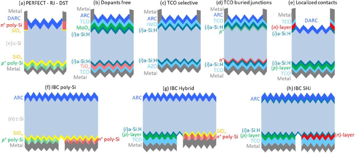
The simulations framework considered different heterojunction (HJT) and TOPCon solar cell architectures based on several CSC designs, including poly-silicon (poly-Si) and dopant-free structures. It also took into account metallization pitch, c-Si thickness, and wafer resistivity, with some of the analyzed cell designs being based on transparent conductive oxide (TCO) or being dopants-free.
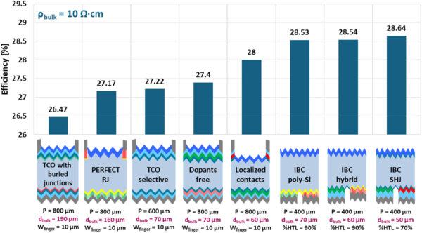
“For IBC designs, with a 400-μm wide pitch and 10 Ω cm wafer resistivity, we calculated maximum efficiencies of 28.53%, 28.54%, and 28.64% in case of IBC poly-Si, IBC Hybrid and IBC SHJ solar cells, respectively,” the academics emphasized. “Our simulation results demonstrate that FBC Localized contacts solar cell and all IBC designs are able to achieve efficiencies equal or higher than 28%.”
They also identified patterning limitations as the main technological barrier determining the intrinsic efficiency limits in FBC and IBC cells, with narrower patterning being pointed out as a potential solution.
“What makes our results insightful for researchers and industries alike is to be able to discern transport mechanisms at play in different c-Si solar cell architectures and technologies. When all CSC approaches deliver both excellent surface passivation and carriers’ selectivity, the usual lifetime and resistivity measurements cannot explain in detail what is going on across contact stacks. Our contribution unveils the interaction between work functions, heterointerface barriers, and energy alignment between materials and crucially optimizes such aspects to achieve ultimate conversion efficiency,” said co-author Olindo Isabella.
This content is protected by copyright and may not be reused. If you want to cooperate with us and would like to reuse some of our content, please contact: editors@pv-magazine.com.


By submitting this form you agree to pv magazine using your data for the purposes of publishing your comment.
Your personal data will only be disclosed or otherwise transmitted to third parties for the purposes of spam filtering or if this is necessary for technical maintenance of the website. Any other transfer to third parties will not take place unless this is justified on the basis of applicable data protection regulations or if pv magazine is legally obliged to do so.
You may revoke this consent at any time with effect for the future, in which case your personal data will be deleted immediately. Otherwise, your data will be deleted if pv magazine has processed your request or the purpose of data storage is fulfilled.
Further information on data privacy can be found in our Data Protection Policy.