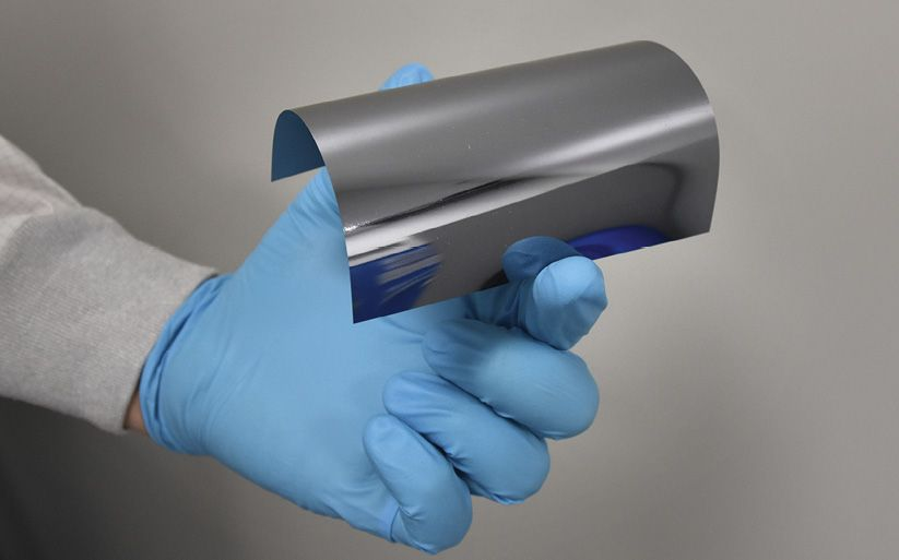
German wafer manufacturer NexWafe GmbH announced it achieved a power conversion efficiency of 24.4% for a heterojunction (HJT) solar cell built with its ultrathin wafers.
The company said the efficiency was achieved with an unspecified M6 HJT commercial production line, without specifying if the results was certified by an independent third party.
“The result confirms that NexWafe's direct gas-to-wafer process is a full replacement for conventional Czochralski (CZ) wafers, while offering the potential for significant cost savings by reducing material losses, energy consumption by 40%, and eliminating the saw damage etching process step in cell production,” it added. “The oxygen content of EpiNex wafers is also 20 times lower than conventional CZ wafers. This enables thermal stability and helps improve cell performance.”
The company also said that a perovskite-silicon tandem solar cell it developed in partnership with the Swiss Center for Electronics and Microtechnology (CSEM) achieved a power conversion efficiency of 28.9%.
The manufacturer claims that its EpiWafers technology could help module producers to achieve dramatically higher degrees of efficiency, without having to upgrade their production lines. It also claims that its technology can enable the production of ultra-thin wafers. It has already demonstrated this on its pilot line in Freiburg, Germany.
NexWafe develops and produces monocrystalline silicon wafers grown directly from inexpensive raw materials. The continuous, direct gas-to-wafer manufacturing process obviates the need for costly and energy-intensive intermediate steps such as polysilicon production and ingot pulling on which traditional wafer manufacturing relies. The process also reportedly minimizes wastage, cutting wafer production costs by up to 30%. It also offers a 70% reduction in carbon dioxide emissions during manufacturing, according to the company.
NexWafe is planning to commission its epitaxial facility in Bitterfeld, in the district of Anhalt-Bitterfeld, Saxony-Anhalt, Germany, by June 2025.
“This innovative system uses advanced heating systems and atmospheric pressure chemical vapor deposition to deposit monocrystalline silicon over an area of 1.3 m x 50 cm, equivalent to more than fourteen G12 wafers in a single pass,” it explained. “With proven deposition rates of 5 microns per minute and temperature uniformity achieving a total thickness variation (TTV) of less than 40%, this platform represents a significant leap in manufacturing scalability.”
This content is protected by copyright and may not be reused. If you want to cooperate with us and would like to reuse some of our content, please contact: editors@pv-magazine.com.


By submitting this form you agree to pv magazine using your data for the purposes of publishing your comment.
Your personal data will only be disclosed or otherwise transmitted to third parties for the purposes of spam filtering or if this is necessary for technical maintenance of the website. Any other transfer to third parties will not take place unless this is justified on the basis of applicable data protection regulations or if pv magazine is legally obliged to do so.
You may revoke this consent at any time with effect for the future, in which case your personal data will be deleted immediately. Otherwise, your data will be deleted if pv magazine has processed your request or the purpose of data storage is fulfilled.
Further information on data privacy can be found in our Data Protection Policy.