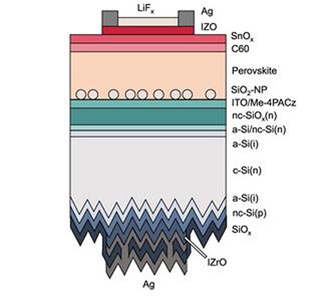
An international group of scientists led by the Ecole Polytechnique Fédérale de Lausanne (EPFL) in Switzerland has developed a perovskite-silicon tandem solar cell integrating a top perovskite cell based on an absorber treated with 2,3,4,5,6-pentafluorobenzylphosphonic acid (pFBPA).
In the study “Synergetic substrate and additive engineering for over 30%-efficient perovskite-Si tandem solar cells,” published in Joule, the researchers said the use of pFBPA is intended to reduce lead-related defects in the perovskite film and the non-radiative recombination near the perovskite absorber and the electron transport layer, thus increasing the cell efficiency and fill factor.
The researchers also explained that the proposed cell configuration and the related manufacturing process eliminate the need for a post-deposition passivation treatment or an additional passivating layer, as the pFBPA was added into the perovskite precursor ink.
The team built the top cell with a substrate made of indium tin oxide (ITO), a hole transport layer (HTL) relying on silicon dioxide (SiO2) nanoparticles and phosphonic acid called methyl-substituted carbazole (Me-4PACz), a perovskite absorber, an ETL based on buckminsterfullerene (C60), a buffer layer made of silicon oxide (SiO2) nanoparticles (NPs), a transparent contact based on indium zinc oxide (IZO), and a silver (Ag) metal contact.
“Similar to PERC cells, the configuration consists of the insulating perovskite/SiO2-NP interface with high-passivation quality and the HTL/perovskite interface through which the current passes and with a passivation quality worse than that achieved with the SiO2-NPs,” the academics explained. “Overall, the results show that care must be taken when optimizing the SiO2-NP concentration, which is affected by the choice of both the HTL and perovskite composition, both of which can influence charge transport at the HTL/perovskite interface.”
The perovskite cell was integrated into a tandem cell with a bottom cell based on heterojunction (HJT) technology and made with a 190-μm-thick, 2 Ω.cm, n-type, float-zone, shiny-etched monocrystalline wafer. “The inverted structure, with the p-type contact at the bottom and n-type at the top, is common for most high-efficiency perovskite-Si devices of today due to the relatively transparent electron transport layers of the perovskite cell and the well-established SHJ technology that requires few modifications to be integrated in tandems,” the group emphasized.
Tested under standard illumination conditions, the tandem device achieved a power conversion efficiency of 30.9%. The scientists said the result was certified by the US Department of Energy's National Renewable Energy Laboratory (NREL). They attributed the remarkable performance of the cell to the gains that can be achieved with pFBPA, especially if used in combination with a SiO2-NP-coated substrate, which they said prevents, in turn, the formation of pinholes and shunts due to the pFBPA use.
“The wettability-enhancing SiO2-NPs also enable the reliable use of high-performance Me-4PACz as an HTL that further reduces the shunt-resistance (Rs) and improves in particular the fill factor of the devices,” they concluded.
*The article was updated on May 27 to reflect that the cell result was certified by the NREL.
This content is protected by copyright and may not be reused. If you want to cooperate with us and would like to reuse some of our content, please contact: editors@pv-magazine.com.


Can you evaluate the performance of this cell after 10 or 25 years? In other words, what is its degradation rate?