From pv magazine Germany
With a new type of laser, wafers can be processed 10 to 20 times faster than before. This is the result of a research project at the Fraunhofer Institute for Solar Energy Systems (Fraunhofer ISE) in Germany.
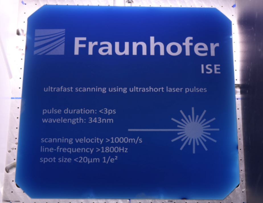
The researchers developed a prototype that can engrave the finest structures in silicon wafers using UV waves. The new system concept enables solar cell manufacturers to carry out laser processing at the highest speed without having to compromise on the size of the structure or processing field.
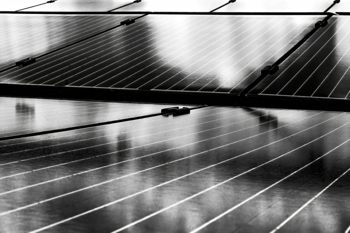
In order to produce photovoltaic cells from wafers, the wafers must, among other things, be metalized. During this step, fine channels are furrowed on the top of the cells. The silver paste goes into the channels and then serves as a conductor track. The speed at which the channels come onto the wafer is very important for the production of cells to further reduce production costs.
The laser presented by Fraunhofer ISE can draw 1800 lines per second. This is 10 to 20 times as fast as a so-called galvanometer scanner, which is often used for this purpose. The laser has a high repetition rate of 10 megahertz and a maximum pulse energy of 5.6 microjoules.
The laser can also process wafers in M12 format with a side length of 210 millimeters. The channels engraved by the laser are just 15 micrometers wide. This is 30 percent finer than current UV wave lasers that are already used commercially. Compared to the very widespread infrared lasers, the channels of the new laser are three times as fine. Finer channels allow for reduced use of silver paste and can thus help further reduce production costs.
“The special thing about the design of the demonstrator is that large workpieces can be processed very quickly and with a small structure size,” said Jale Schneider, project manager at Fraunhofer ISE. “A large image field, fast processing, fine structures – the idea that you can only have two of these three properties at the same time is firmly anchored in the laser material processing industry. With this system, we have fulfilled all three wishes at the same time.”
German laser specialist Edgewave GmbH developed the prototype. Moewe Optical Solutions built a polygon scanner for the project. At Fraunhofer ISE, the team put together the polygon scanner, the laser and an axis for beam guidance into a system. The group now wants to look at new processes to increase throughput.
This content is protected by copyright and may not be reused. If you want to cooperate with us and would like to reuse some of our content, please contact: editors@pv-magazine.com.


By submitting this form you agree to pv magazine using your data for the purposes of publishing your comment.
Your personal data will only be disclosed or otherwise transmitted to third parties for the purposes of spam filtering or if this is necessary for technical maintenance of the website. Any other transfer to third parties will not take place unless this is justified on the basis of applicable data protection regulations or if pv magazine is legally obliged to do so.
You may revoke this consent at any time with effect for the future, in which case your personal data will be deleted immediately. Otherwise, your data will be deleted if pv magazine has processed your request or the purpose of data storage is fulfilled.
Further information on data privacy can be found in our Data Protection Policy.