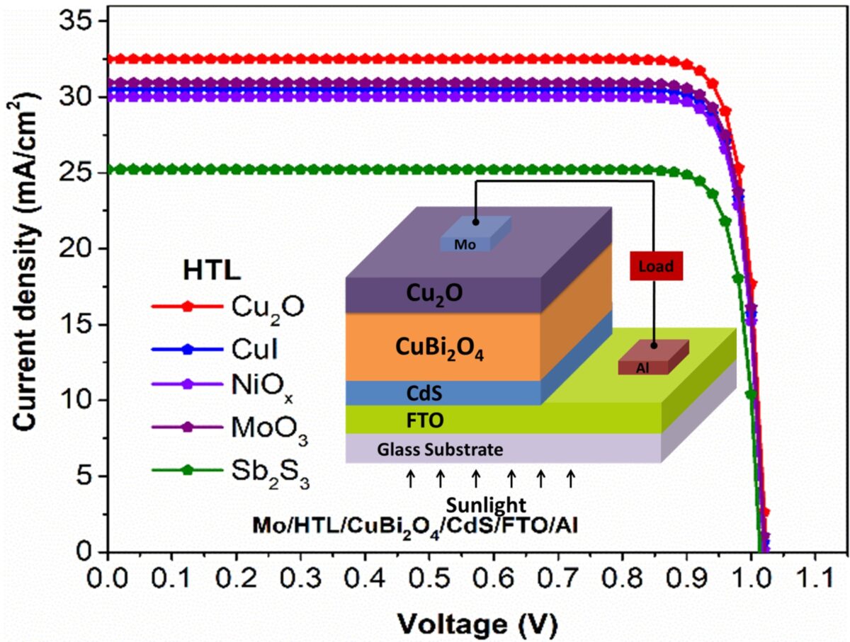
Researchers at the Pabna University of Science and Technology, in Bangladesh, have developed a new architecture for thin-film solar cells based on copper bismuth oxide (CuBi2O4).
CuBi2O4 is an abundant, inexpensive, and harmless p-type semiconductor that has been recently identified as a photocathode with a two-dimensional porous heterojunction structure. “CuBi2O4 thin films can be fabricated based on the solution process by using a simple and low-cost spin coating technique,” research co-author, Sheikh Rashel Al Ahmed, told pv magazine. “This material also has several advantages such as suitable bandgap, minimal toxicity, chemical stability, abundant organic compounds, and affordable processing.”
In the paper “Design and simulation of a highly efficient CuBi2O4 thin-film solar cell with hole transport layer,” published in Optics & Laser Technology, Al Ahmed and his group used the SCAPS-1D solar cell capacitance software, developed by the University of Ghent, to simulate a novel cell configuration based on various hole transport layers (HTLs). The same research group unveiled in 2021 a heterojunction design for CuBi2O4 that didn't consider the use of an HTL.
The new cell developed by the scientists is based on a glass substrate coated with molybdenum (Mo), and HTL made of copper(I) oxide (Cu2O), the CuBi2O4 absorber, a cadmium sulfide (CdS) buffer layer, a fluorine-doped tin oxide (FTO) layer, and an aluminum (Al) metal contact. The academics inserted the HTL at the rear side of the absorber.
“The inclusion of HTL may improve the carrier gathering by the electrodes,” the researchers stated. “In addition, holes enter the contact layer as electrons are effectively returned to the n-type space charge area. As a result, in the p-type area, the minority carrier recombination loss diminishes.”
The group conducted a computational analysis to assess the effect of the absorber bulk defects on the cell performance.
The simulated cell achieved a power conversion efficiency of 29.2%, an open-circuit voltage of 1.02 V, a short-circuit current density of 32.49 mA/cm2, and a fill factor of 87.91%.
“The addition of HTL was effective in decreasing the absorber thickness in the solar cell with significant PV performances by minimizing the carrier recombination loss at the back surface,” Al Ahmed said. “Thus, the thinner absorber layer in the solar cells allows to reduce the required amounts of raw material and hence reduces the total manufacturing cost of the thinner CuBi2O4 TFSC with the introduction of Cu2O HTL.”
“The entire evaluation process with the present approach will give important evidence of design complexity in the solar cells for the scientists, consequently decreasing the fabrication cost, time, and difficulty considerably,” he concluded.
This content is protected by copyright and may not be reused. If you want to cooperate with us and would like to reuse some of our content, please contact: editors@pv-magazine.com.


1 comment
By submitting this form you agree to pv magazine using your data for the purposes of publishing your comment.
Your personal data will only be disclosed or otherwise transmitted to third parties for the purposes of spam filtering or if this is necessary for technical maintenance of the website. Any other transfer to third parties will not take place unless this is justified on the basis of applicable data protection regulations or if pv magazine is legally obliged to do so.
You may revoke this consent at any time with effect for the future, in which case your personal data will be deleted immediately. Otherwise, your data will be deleted if pv magazine has processed your request or the purpose of data storage is fulfilled.
Further information on data privacy can be found in our Data Protection Policy.