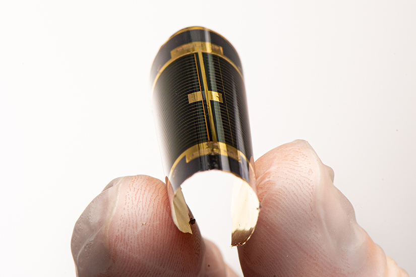
Researchers at the US Department of Energy's National Renewable Energy Laboratory have fabricated a III-V gallium arsenide (GaAs) solar cell based on a substrate made of spalled GaAs.
The cost of producing solar cells based on compounds of III-V element materials, named according to the groups of the periodic table that they belong to, has confined these devices to niche applications, such as drones and satellites, where low weight and high efficiency are more pressing concerns than the cost of energy produced.
“Reducing manufacturing costs is considered key to terrestrial applications, and one way to accomplish this is by having the ability to repeatedly reuse the substrate upon which the cells are grown,” noted the researchers. This was the motivation to develop acoustic spalling, a new process which they claim represents a low-cost reuse pathway for III–V epitaxial growth substrates with recovery and reuse of the substrate.
In the paper “GaAs solar cells grown on acoustically spalled GaAs substrates with 27% efficiency,” which was recently published in Joule, the researchers explained that the acoustic spalling, which is also known as a sonic lift-off (SLO), is an experimental process that utilizes sound waves to control the propagation of the crack tip during the spall in order to suppress facet formation and improve surface flatness.
“Existing technology uses a sacrificial etch layer, which allows a cell to be lifted off a gallium arsenide (GaAs) substrate so that the substrate can be used again, but the process takes hours and leaves behind a residue that requires a polishing step,” the group explained. “Polishing is relatively expensive and limits the potential cost savings of this substrate reuse method. In contrast, spalling takes seconds, creating a controlled fracture within the substrate nearly parallel to its surface. This fracture allows the cell to be easily removed, revealing a new, contaminant-free surface from within the substrate that does not require polishing.”
The academics built PV devices with an n-i-p structure and a 1 mm-thick emitter made of GaAs and selenium (SE), a 1 mm unintentionally doped GaAs layer, and a 1 mm base layer made of GaAs and zinc (Zn) on an as-spalled SLO substrate without wet etching.
Tested under standard illumination conditions, the champion device fabricated with this architecture achieved a certified power conversion efficiency of 26.9%, an open-circuit voltage of 1.061 V, a short-circuit current of 29.9 mA/cm2, and a fill factor of 84.9%, with the cell exhibiting no signs of non-linear shunting, which reduces the current flowing through the solar cell junction and reduces the voltage from the solar cell.
“These results enable the epitaxial growth of high-performance devices on potentially lower-cost substrates with mm-scale features,” the researchers said, adding that the acoustic spalling utilized for building the cells was developed at Arizona State University and is now being commercialized by Phonenix-based startup Crystal Sonic Inc. “This latest advancement uses acoustic spalling, or sound waves, to control the fracture, suppress the formation of facets, and improve the flatness of the substrate.
In July 2022, other researchers from the NREL developed a III-V solar cell based on a substrate made of spalled germanium (Ge). They used spalled Ge instead of gallium arsenide (GaAs), as the former, which is commonly used in space applications, reportedly reduces several issues associated with GaAs spalling.
This solar cell was able to achieve a power conversion efficiency of 23.36% where no spalling defects were present. It also achieved an open-circuit voltage of 1.019 V, a short-circuit current density of 28.49 mA cm−2, and a fill factor of 80.45%. According to the scientists, these results show that spalled germanium does not need to be returned to a pristine, polished state to achieve high-quality device performance.
This content is protected by copyright and may not be reused. If you want to cooperate with us and would like to reuse some of our content, please contact: editors@pv-magazine.com.


By submitting this form you agree to pv magazine using your data for the purposes of publishing your comment.
Your personal data will only be disclosed or otherwise transmitted to third parties for the purposes of spam filtering or if this is necessary for technical maintenance of the website. Any other transfer to third parties will not take place unless this is justified on the basis of applicable data protection regulations or if pv magazine is legally obliged to do so.
You may revoke this consent at any time with effect for the future, in which case your personal data will be deleted immediately. Otherwise, your data will be deleted if pv magazine has processed your request or the purpose of data storage is fulfilled.
Further information on data privacy can be found in our Data Protection Policy.