An international research team has designed a copper indium gallium diselenide (CIGSe) solar cell based on an ultrathin aluminum-doped zinc oxide (AZO) film with strong sheet resistance.
“We employed a low power deposition method for the production of AZO and i-ZnO/AZO bilayer structures used in the cell,” the research's corresponding author, Ganesh Regmi, told pv magazine, noting that this approach is intended at improving the cell efficiency and durability. “By utilizing this technique, the aim is to avoid raising the substrate temperature, which could lead to adverse effects such as atom implantation into the cadmium sulfide (CdS) layer and potential short-circuiting.”
The scientists said this technique eliminates the need for post-deposition treatment, a customary practice in conventional methods that can negatively impact the integrity of the solar cell layers. “In traditional high-efficiency CIGS thin-film solar cells, a relatively thick ZnO layer , with a thickness of 200−300 nm, is commonly employed as the window layer,” Regmi explained. “However, this approach restricts the flexibility of the solar cells, rendering them unsuitable for certain applications.”
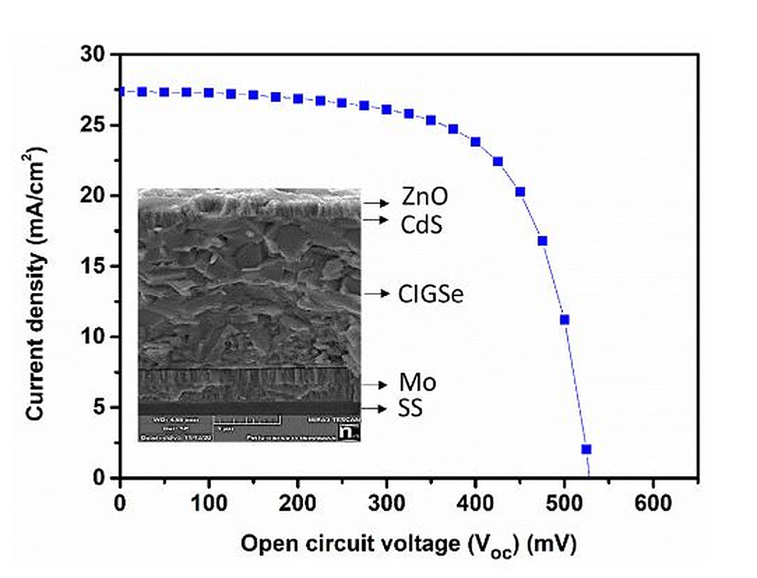
The group built the cell with a monolayer made of molybdenum (Mo), the CIGSe absorber, a cadmium sulfide (CdS) buffer layer, a window layer of zinc oxide (i-ZnO), and a zinc oxide (ZnO) film. The device achieved a power conversion efficiency of 9.53%, an open-circuit voltage of 530 mV, and short-circuit current density of 27.34 mA/cm2, and a fill factor of 65.78%.
The academics claimed that the AZO films exhibited good transmittance and well-crystalline morphology, as well as remarkable electrical conductivity. “This outcome validates the successful implementation of the proposed methods and provides evidence of the potential viability of this approach,” Regmi stated.
They described the device in the study “Aluminum-doped zinc oxide (AZO) ultra-thin films deposited by radio frequency sputtering for flexible Cu(In,Ga)Se2solar cells,” published in Memories – Materials, Devices, Circuits and Systems. The group includes scientists from the Center for Research and Advanced Studies of the National Polytechnic Institute (Cinvestav) in Mexico and the Tribhuvan University in Nepal.
This content is protected by copyright and may not be reused. If you want to cooperate with us and would like to reuse some of our content, please contact: editors@pv-magazine.com.


1 comment
By submitting this form you agree to pv magazine using your data for the purposes of publishing your comment.
Your personal data will only be disclosed or otherwise transmitted to third parties for the purposes of spam filtering or if this is necessary for technical maintenance of the website. Any other transfer to third parties will not take place unless this is justified on the basis of applicable data protection regulations or if pv magazine is legally obliged to do so.
You may revoke this consent at any time with effect for the future, in which case your personal data will be deleted immediately. Otherwise, your data will be deleted if pv magazine has processed your request or the purpose of data storage is fulfilled.
Further information on data privacy can be found in our Data Protection Policy.