An international research group led by Switzerland's Ecole Polytechnique Fédérale de Lausanne (EPFL) has looked at the electrical properties of zinc phosphide (fZn3P2), in another attempt to consider its use as an absorber material in solar cells. So far, cells based on fZn3P2 have reached a very limited power conversion efficiency, due to the intrinsic limitations of their electrical properties, such as minority carrier mobility and carrier diffusion lengths.
The scientists described their findings in “Zn/P ratio and microstructure defines carrier density and electrical transport mechanism in earth-abundant Zn3-xP2+y thin films,” which was recently published in Solar Energy Materials and Solar Cells. They assessed the electrical properties, as well as the chemical composition and microstructure, of polycrystalline and monocrystalline Zn3P2 thin films grown on indium phosphide (InP) substrates.
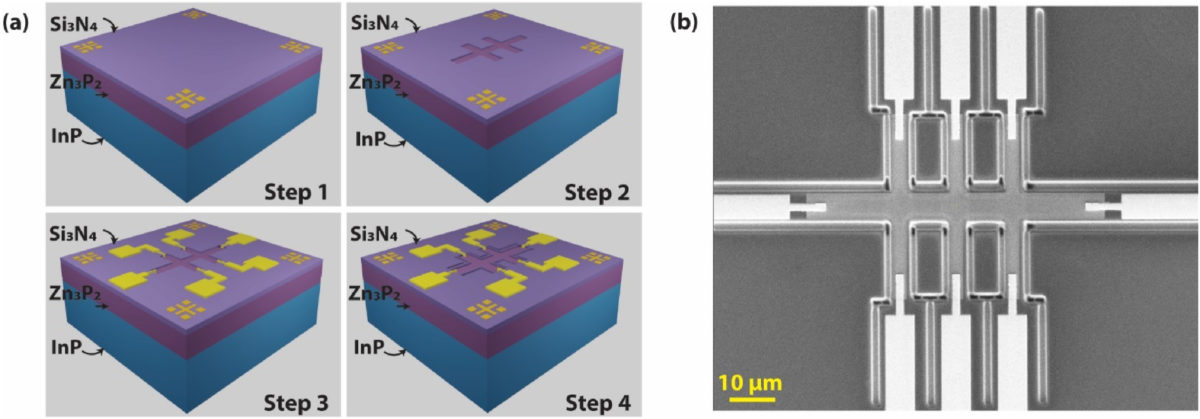
“We demonstrate a device fabrication technique that circumvents challenges arising from micro-cracks present in monocrystalline thin films,” they said. “Temperature-dependent measurements elucidated the defect states and their contribution to the transport in Zn3P2 thin films. We thus show that the growth conditions play a vital role in determining the electrical properties of the given thin films.”
The group fabricated multiple electrical devices based on thin films grown either on doped (both n-and p-type) and undoped InP substrates. They compared their performance with regard to the current-voltage characteristic of Zn3P2/InP heterojunction. They deposited the Zn3P2 films via plasma-enhanced chemical vapor deposition (PECVD).
The academics found that the poly-Zn3P2 thin film has a rough top surface, while the mono-Zn3P2 thin film has a smooth cross-sectional morphology and relatively flat top surface. They also determined that the mono-Zn3P2 thin film has resistivity values in the range of 150 Ω cm to 1,050 Ω cm and the former in the range of 6,500 Ω cm to 9,000 Ω cm.
“The vast difference in resistivity value can be attributed to the presence of grain boundaries in the poly-Zn3P2 thin films, which could contribute to increased scattering of the charge carriers,” the scientists explained.
Additional analysis showed that the mono-Zn3P2 film could achieve higher current density values in comparison to the poly-Zn3P2 device. The researchers attributed the lower current density value of the polycrystalline thin film to the high resistivity in the material.
“High-quality monocrystalline Zn3P2 thin films with moderate carrier concertation demonstrated a high hole mobility (125 cm2/Vs) at room temperature, indicating the growth conditions and composition of the material play an integral role in tuning the material functionality,” the researchers said. “We unveiled the impact of unintentional doping caused due changes in the Zn/P ratio on the electrical properties of the material.”
Their conclusion is that the carrier concentration in the devices is directly correlated to the Zn/P ratio.
“This work sheds light on the electrical properties and conduction mechanism, thus providing a better understanding of the limitations and potentials of the electrical devices related to the material,” said the researchers.
The team includes scientists from Universidad de Salamanca in Spain.
This content is protected by copyright and may not be reused. If you want to cooperate with us and would like to reuse some of our content, please contact: editors@pv-magazine.com.


By submitting this form you agree to pv magazine using your data for the purposes of publishing your comment.
Your personal data will only be disclosed or otherwise transmitted to third parties for the purposes of spam filtering or if this is necessary for technical maintenance of the website. Any other transfer to third parties will not take place unless this is justified on the basis of applicable data protection regulations or if pv magazine is legally obliged to do so.
You may revoke this consent at any time with effect for the future, in which case your personal data will be deleted immediately. Otherwise, your data will be deleted if pv magazine has processed your request or the purpose of data storage is fulfilled.
Further information on data privacy can be found in our Data Protection Policy.