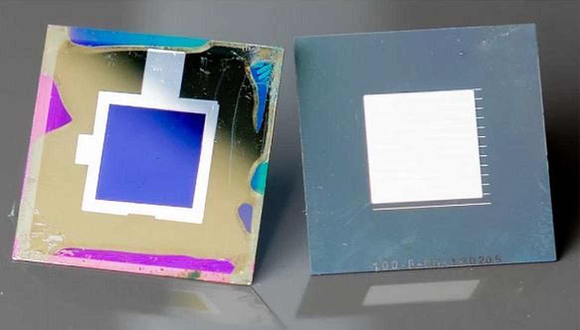
A research group led by German research institute Helmholtz-Zentrum Berlin für Materialien und Energie GmbH has demonstrated a tandem perovskite-silicon solar cell based on submicrometre-periodic nanotextures and an improved back-reflector design.
In the study “Nano-optical designs for high-efficiency monolithic perovskite–silicon tandem solar cells,” published in nature nanotechnology, the scientists explained that the gentle sinusoidal nanotexture that they used in the cell combines the advantages of structuring the silicon surface with maintaining high material quality of the solution-processed perovskite.
“We show that the nanotexturing causes a substantial reduction of reflection losses compared to their planar counterpart, strongly improves the fabrication yield enabled by the excellent film formation properties and increases the open-circuit voltage by 15 mV,” they stated.
By using ultraviolet nanoimprint lithography, reactive ion etching and wet chemical etching, the German group built the cell with a reflector with a dielectric buffer layer (RDBL) at the rear side of the silicon bottom cell and a sinusoidal nanostructure at the front surface.
The team designed the tandem device with a passivated contact made with a layer of hydrogenated nanocrystalline silicon carbide (nc-SiC:H(n)), doped indium oxide as the transparent conducting oxide (TCO), a self-assembled monolayer of methyl-substituted carbazole (Me-4PACz) as the hole-transport layer, and a perovskite absorber. The silicon silicon bottom cell has a size of 2.5 × 2.5 cm2 and a 1.1 cm2 contact area in the center.
“The RDBL comprises a silicon oxide (SiO2) buffer layer between the TCO and the silver back-reflector, reducing parasitic absorption losses. A silver grid covering 4% of the active area is screen-printed on top of the TCO before SiO2 deposition to establish the electric contact between the TCO and Ag,” they further explained.
Experts from Germany's Fraunhofer ISE CalLab tested the performance of the solar cell and certified that it achieved a power conversion efficiency of 29.80%, an open-circuit voltage of 1.92 V, a short-circuit current of 19.56 mA cm−2, and a fill factor of 79.4%. The scientists said these short-circuit current levels, for both the perovskite top cell and the silicon bottom cell, are among the highest values reported in the literature for two-terminal tandem perovskite-silicon cells to date.
“A sensitivity analysis further indicates that the nanotextures substantially improve the performance robustness upon deviations from the optimal nanocrystalline silicon oxide layer thickness — an important aspect with regards to the industrialization of tandem technology and processing on larger areas,” they concluded.
This content is protected by copyright and may not be reused. If you want to cooperate with us and would like to reuse some of our content, please contact: editors@pv-magazine.com.


2 comments
By submitting this form you agree to pv magazine using your data for the purposes of publishing your comment.
Your personal data will only be disclosed or otherwise transmitted to third parties for the purposes of spam filtering or if this is necessary for technical maintenance of the website. Any other transfer to third parties will not take place unless this is justified on the basis of applicable data protection regulations or if pv magazine is legally obliged to do so.
You may revoke this consent at any time with effect for the future, in which case your personal data will be deleted immediately. Otherwise, your data will be deleted if pv magazine has processed your request or the purpose of data storage is fulfilled.
Further information on data privacy can be found in our Data Protection Policy.