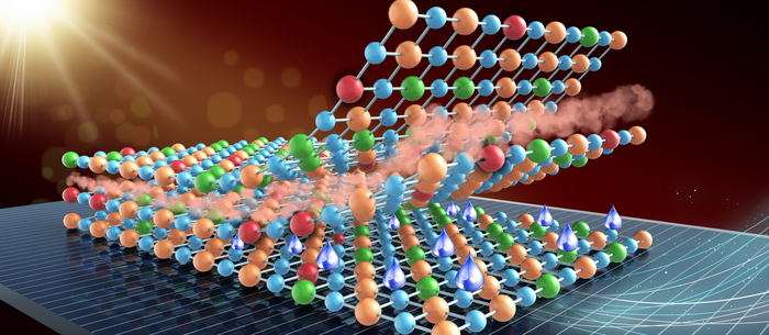
When working with perovskite solar cells, improvements to stability often come with a cost to performance, and vice-versa. Finding the right balance between the two is an important goal for scientists in this field. And since the perovskite structure is versatile in both the materials it can contain and the ways it can be produced as a thin-film solar cell, there is a wealth of different approaches under investigation.
Among these is the “inverted” perovskite cell, where the perovskite cell material is deposited onto a hole transport layer, and then coated with an electron transport layer – the opposite way round to conventional device architecture. Inverted perovskite solar cells typically show strong stability, but have lagged behind conventional devices in terms of conversion efficiency and cell performance.
A group of scientists led by China’s Dalian Institute of Chemical Physics is now looking to improve performance without losing the stability advantage, primarily through surface engineering of the hole transport layer onto which the perovskite is deposited. The group worked with nickel oxide (NiOx) for the hole transport layer (HTL), which previous work has shown to have excellent stability and light transmittance, but is also prone to problems at the interface between perovskite material and HTL, particularly when devices are scaled to a larger size.
By engineering the surface of the HTL before the perovskite was applied using slot-die coating, the group was able to improve various characteristics including uniformity of the perovskite film and mechanical adhesion at the interface. The group described the approach in the paper “Surface redox engineering of vacuum-deposited NiOx for top-performance perovskite solar cells and modules,” published in Joule.
It was able to demonstrate small-size perovskite solar cells that reached conversion efficiencies of 23.4% (rigid device) and 21.3% (flexible). And when scaled up to a larger area of 156 mm x 156 mm – similar to that of a crystalline silicon cell – the approach maintained efficiency of 18.6%. The group did not share stability figures, but stated that each device maintained high performance after “thousands of hours under various stressed conditions.”
“The SRE strategy provides a proof of concept for combining vacuum-fabricated charge transport layers with wet-processed perovskites and facilitates the stacking engineering of large-scale, uniform thin films for the development of efficient and stable perovskite modules,” said Liu Shengzhong, a scientist with the Dalian Institute who led this research.
This content is protected by copyright and may not be reused. If you want to cooperate with us and would like to reuse some of our content, please contact: editors@pv-magazine.com.


By submitting this form you agree to pv magazine using your data for the purposes of publishing your comment.
Your personal data will only be disclosed or otherwise transmitted to third parties for the purposes of spam filtering or if this is necessary for technical maintenance of the website. Any other transfer to third parties will not take place unless this is justified on the basis of applicable data protection regulations or if pv magazine is legally obliged to do so.
You may revoke this consent at any time with effect for the future, in which case your personal data will be deleted immediately. Otherwise, your data will be deleted if pv magazine has processed your request or the purpose of data storage is fulfilled.
Further information on data privacy can be found in our Data Protection Policy.