While it is now widely accepted that the question for perovskite solar cells in mass production is “not if, but when”, a wealth of different approaches to the material is still being explored by researchers the world over and its far from clear which type of device will ultimately bring the best performance of performance, stability and manufacturability.
Among these approaches are inverted perovskite devices, where the negative electrode is placed at the top layer of the cell, and the positive at the bottom – as opposed to the typical device where this is reversed. This approach has shown strong stability performance and could potentially open up new manufacturing techniques for exploration, but it also comes with challenges. “It’s hard to get good contact between the perovskite layer and the top electrode,” says Hao Chen, a post-doctoral researcher at the University of Toronto. “To solve this, researchers typically insert a passivation layer made of organic molecules. That works really well in the traditional orientation, because ‘holes’ can go right through this passivation layer. But electrons are blocked by this layer, so when you invert the cell it becomes a big problem.”
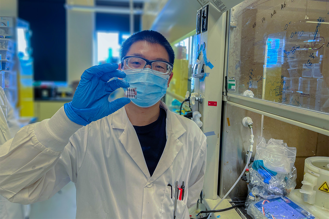
Overcoming this challenge to the electron flow was the goal of Chen and his colleagues, who worked with extremely thin “two-dimensional” perovskite layers, which afforded them better control over the material’s “quantum mechanics” characteristics – those that differ from the material’s overall behavior when observed at a larger scale, such as the movement of electrons or absorption of particular wavelengths of light. By slightly increasing the thickness of the layer, from one to three crystals in height, more electrons were able to escape through the passivation layer and into a circuit.
The research is described in full in a paper published in Nature Photonics. Cells fabricated by the group achieved 23.9% efficiency, which did not fade after the devices were left unencapsulated in ambient conditions for 1,000 hours. The cells were also encapsulated and subjected to harsher accelerated aging tests, where they retained 92% of initial performance after 500 hours.
The group says that its future work will focus on improving this stability performance, as well as scaling up the approach to larger area devices than the 5mm² used for these cells. “We compare our prototypes to both traditional and inverted perovskite solar cells that have been recently published in the scientific literature,” said researcher Sam Teale. “The combination of high stability and high efficiency we achieved really stands out. We should also keep in mind that perovskite technology is only a couple of decades old, whereas silicon has been worked on for 70 years. There are a lot of improvements still to come.”
This content is protected by copyright and may not be reused. If you want to cooperate with us and would like to reuse some of our content, please contact: editors@pv-magazine.com.


2 comments
By submitting this form you agree to pv magazine using your data for the purposes of publishing your comment.
Your personal data will only be disclosed or otherwise transmitted to third parties for the purposes of spam filtering or if this is necessary for technical maintenance of the website. Any other transfer to third parties will not take place unless this is justified on the basis of applicable data protection regulations or if pv magazine is legally obliged to do so.
You may revoke this consent at any time with effect for the future, in which case your personal data will be deleted immediately. Otherwise, your data will be deleted if pv magazine has processed your request or the purpose of data storage is fulfilled.
Further information on data privacy can be found in our Data Protection Policy.