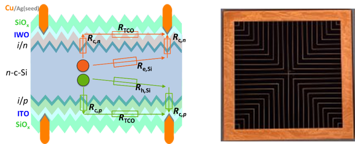
An international research group has achieved a 22% power conversion efficiency in a bifacial heterojunction crystalline solar cell fabricated with reduced thickness for the transparent conductive oxide (TCO).
“The work is intended for sustainable PV development, with reducing scarce material use, meanwhile improving solar cell performance,” researcher Olindo Isabella told pv magazine. “Beside bifacial silicon heterojunction devices, the results of this study could provide insights in the development of other TCO-required c-Si solar cells with carrier selective passivating contacts, such as high-efficiency bifacial TOPCon, and metal oxide-based contacts.”
The TCOs used for the cell are based on indium(III) oxide (In2O3), which is considered a technology-critical element by many experts.
“Reducing indium consumption, which is related to the transparent conductive oxide (TCO) use, is a key challenge for scaling up silicon heterojunction (SHJ) solar cell technology to terawatt level,” the scientists said.
They tested three types of indium oxides doped with tin (ITO), fluorine (IFO), and tungsten (IWO). The three oxides exhibited different opto-electrical properties from post-transition metallic cationic doping, anionic doping, and transition metallic cationic doping, respectively.
They deposited the oxides on corning glass substrates at room temperature through the radio frequency (RF) magnetron sputtering technique, which is an approach involving alternating the electrical potential of the current in a vacuum environment at RFs. The 2 cm2 × 2 cm2 cell was fabricated via copper (Cu) plating metallization, based on a technique that was recently developed by the same research group.
“Silver consumption is largely reduced due to the use of copper-plating metallization approach,” Isabella further said.
The properties of the three TCOs were assessed through an HMS-5000 Hall Effect Measurement System provided by South Korea-based Ecopia Corp. and an M-2000 DI spectroscopic ellipsometer supplied by US-based J. A. Woollam. The measurements showed the IFO and IWO are favorable for p-contact and n-contact, respectively, while the ITO was found to work well in both p-contact and n-contact.
The performance of the solar cells was analyzed for both monofacial and bifacial SHJ devices. The champion solar cell is a 22.84%-efficient bifacial device built with a 25 nm-thick IWO on the front side and 25-nm-thick ITO on the rear side.
“This represents a 67% TCO reduction with respect to a reference bifacial solar cell with 75-nm-thick TCO on both sides,” the scientists said.
The scientists described the manufacturing technique in “Towards bifacial silicon heterojunction solar cells with reduced TCO use,” which was recently published in Progress in Photovoltaics. The research group includes scientists from the Delft University of Technology (TU Delft) in the Netherlands and Nankai University in China.
This content is protected by copyright and may not be reused. If you want to cooperate with us and would like to reuse some of our content, please contact: editors@pv-magazine.com.


4 comments
By submitting this form you agree to pv magazine using your data for the purposes of publishing your comment.
Your personal data will only be disclosed or otherwise transmitted to third parties for the purposes of spam filtering or if this is necessary for technical maintenance of the website. Any other transfer to third parties will not take place unless this is justified on the basis of applicable data protection regulations or if pv magazine is legally obliged to do so.
You may revoke this consent at any time with effect for the future, in which case your personal data will be deleted immediately. Otherwise, your data will be deleted if pv magazine has processed your request or the purpose of data storage is fulfilled.
Further information on data privacy can be found in our Data Protection Policy.