Though many more potential solar cell materials have been discovered, and in some cases successfully commercialized, silicon continues to represent the vast majority of the market for solar energy products.
Thanks to its relative abundance and its importance to the semiconductor industry, silicon is still the most practical material to work with in large-scale production of solar cells. The structure of a silicon cell, however, means light is absorbed through an ‘indirect bandgap’ – meaning the material is relatively inefficient at absorbing sunlight.
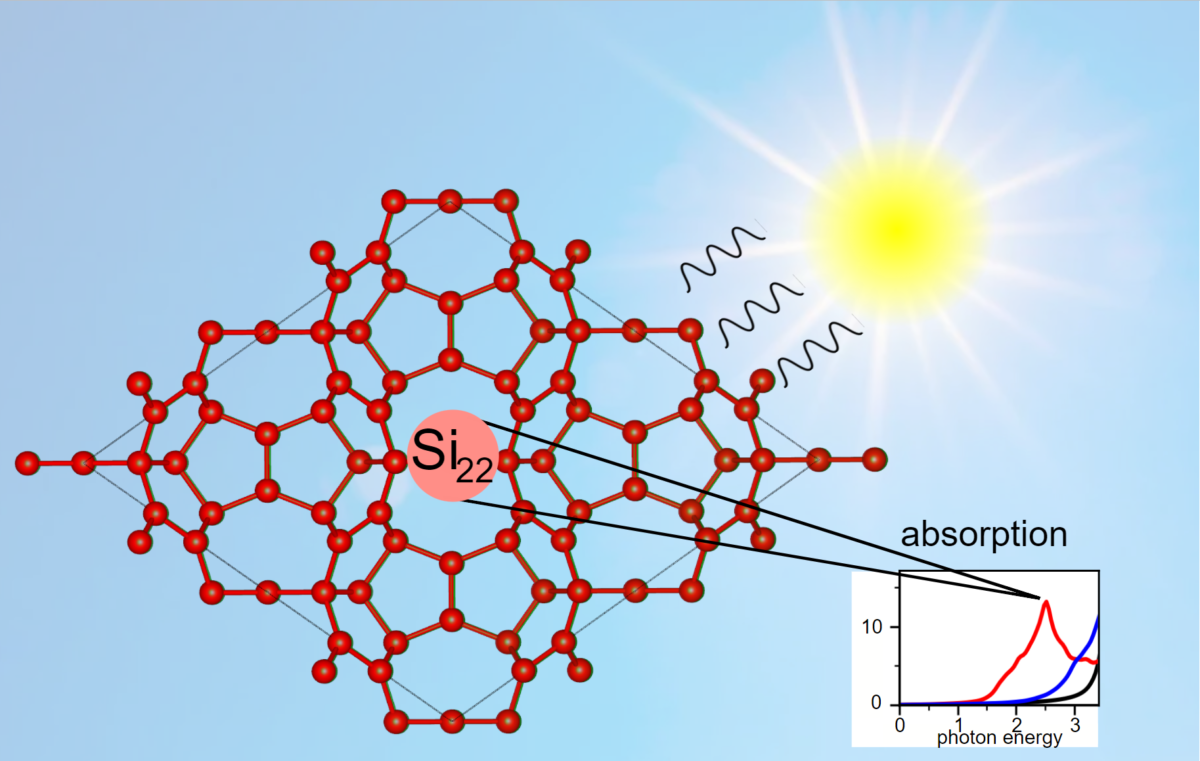
A group of scientists led by the US Department of Energy's Los Alamos National Laboratory has theorized that by altering the structure of silicon to create an allotrope – the same element in the same state, but with a different atomic structure – they could improve its light-absorbing characteristics, and performance as a solar cell.
The calculations are described in full in the paper Exceptional Radiation Absorption in a Pentagon-Based Si Allotrope, published in Nano Letters. In the allotrope, Si22, silicon atoms are arranged into a network of hollow, pentagonal structures. The structure is said to be thermally and dynamically stable, and able to directly absorb visible frequencies of light.
Multiple possibilities
Aside from solar cells, the group also calculated that, thanks to the way it vibrates and its performance at very low temperatures, the allotrope could be a useful material for work in quantum computing.
The hollow structure could also be useful in incorporating other atoms – making it potentially interesting in energy storage applications, as well as in carbon sequestration – where the silicon structure would hold carbon atoms within it, keeping them out of the atmosphere.
The properties of this silicon allotrope, however, have so far only been calculated theoretically, and much more work will be required to confirm the behavior and the potential of this material in the ‘real world’. “[This research] has laid a foundation for the potential of the new material, and experimentation would need to follow up to further test the material’s properties,” reads a statement from LANL. “Designing and understanding the properties of the new material is the first step, and the first step is taken.”
*this article was amended on 08/11 to correct an error: The research was published in Nano Letters, not Nano Energy as previously stated.
This content is protected by copyright and may not be reused. If you want to cooperate with us and would like to reuse some of our content, please contact: editors@pv-magazine.com.


3 comments
By submitting this form you agree to pv magazine using your data for the purposes of publishing your comment.
Your personal data will only be disclosed or otherwise transmitted to third parties for the purposes of spam filtering or if this is necessary for technical maintenance of the website. Any other transfer to third parties will not take place unless this is justified on the basis of applicable data protection regulations or if pv magazine is legally obliged to do so.
You may revoke this consent at any time with effect for the future, in which case your personal data will be deleted immediately. Otherwise, your data will be deleted if pv magazine has processed your request or the purpose of data storage is fulfilled.
Further information on data privacy can be found in our Data Protection Policy.