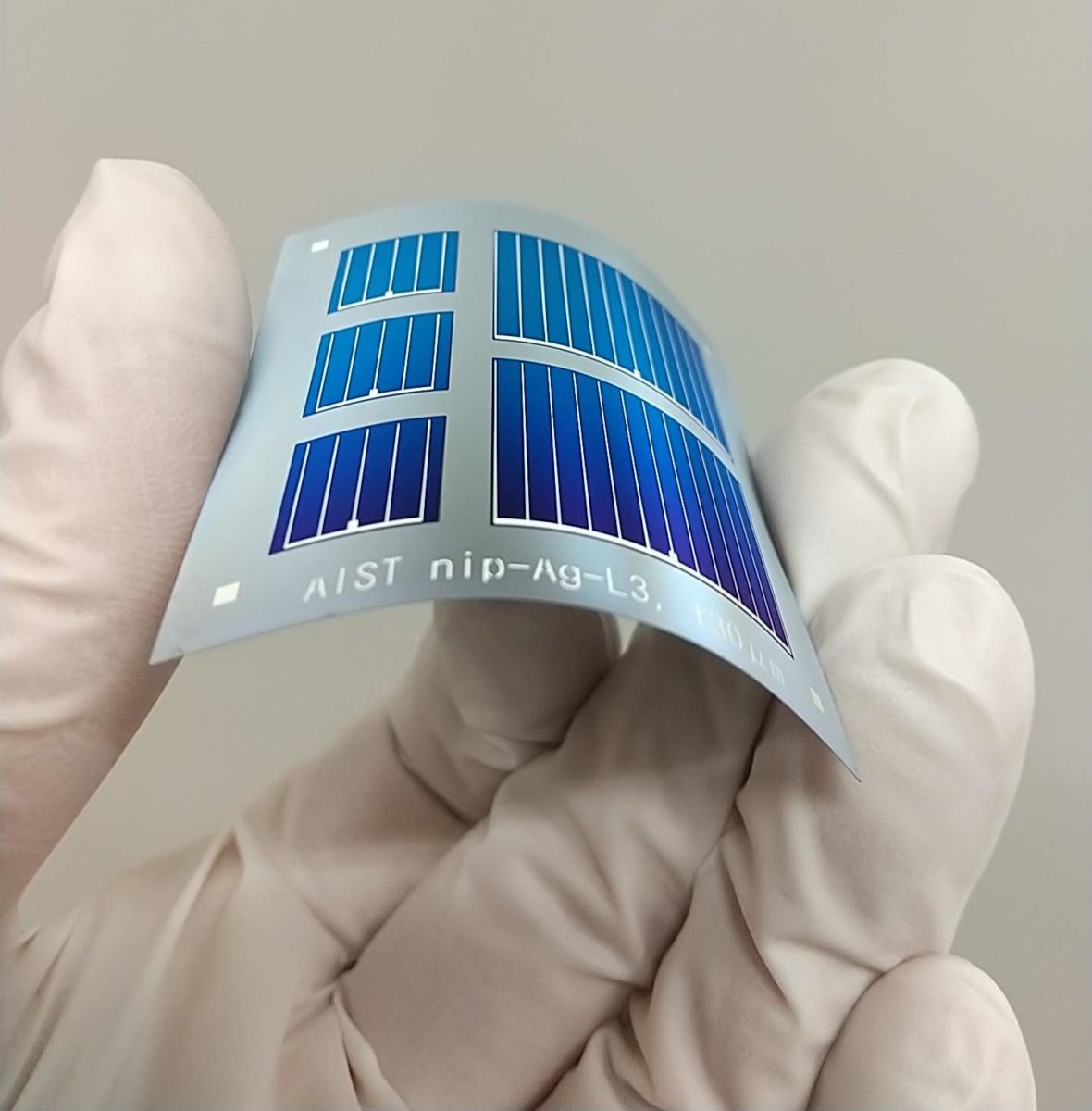
A group of scientists from Japan’s National Institute of Advanced Industrial Science and Technology (AIST) has developed an ultra-thin heterojunction solar cell for application in lightweight, flexible solar modules.
“Building thinner devices is beneficial for reducing the material costs,” the research's main author, Hitoshi Sai, told pv magazine. “There are several issues to be tackled for the commercial production of very thin c-Si cells, but our results encourage [progression] to thinner wafers, with a size of 120μm, from the current industry standard of 160μm.”
The solar cell has an area of 4cm2 and was fabricated with an n-type Czochralski (CZ)-grown monocrystalline silicon wafer with a thickness of only 56.2μm. The scientists decided to replace the hydrogenated amorphous silicon (a-Si:H) layer that is commonly used in this kind of cell with a hydrogenated nanocrystalline silicon (nc-Si:H) layer, which is said to show improved surface passivation, lower parasitic absorption, and higher external quantum efficiency. The layer was grown through plasma-enhanced chemical vapor deposition (PECVD).
An anti-reflecting coating based on silicon oxide (SiOx) was also applied on the cell surface to reduce primary reflection loss. The device was tested under standard illumination conditions and was found to exhibit a power conversion efficiency of 23.27%. It also showed an open-circuit voltage of 754 mV, a short-circuit current of 37.85 mA/cm2, and a fill factor of 81.5%.
“To our knowledge, the open-circuit voltage of 754 mV is the highest value independently confirmed under standard test conditions among any c-Si solar cells reported so far, even though the size of our SHJ [silicon heterojunction] cell is small,” the researchers stated, noting that 23.27% efficiency is also the highest value for c-Si solar cells with a thickness of less than 60μm.
According to the Japanese group, the device's high open-circuit voltage is beneficial for its power yield, as it helps mitigate performance
degradation at elevated temperatures, which makes the cell particularly suitable for hot and sunny climate regions. “Needless to say, the mass production of very thin c-Si cells and modules with a sufficient yield and a high throughput, remains a challenging issue,” they also acknowledged.
The scientists concluded that their new cell demonstrates that the heterojunction architecture can be successfully used also with ultra-thin solar cells, and that this configuration offers the advantage of superior surface passivation combined with a manufacturing process which can be carried out at lower temperature.
The device was described in the study Very Thin (56 μm) Silicon Heterojunction Solar Cells with an Efficiency of 23.3% and an Open-Circuit Voltage of 754 mV, which was recently published in RRL Solar.
This content is protected by copyright and may not be reused. If you want to cooperate with us and would like to reuse some of our content, please contact: editors@pv-magazine.com.


1 comment
By submitting this form you agree to pv magazine using your data for the purposes of publishing your comment.
Your personal data will only be disclosed or otherwise transmitted to third parties for the purposes of spam filtering or if this is necessary for technical maintenance of the website. Any other transfer to third parties will not take place unless this is justified on the basis of applicable data protection regulations or if pv magazine is legally obliged to do so.
You may revoke this consent at any time with effect for the future, in which case your personal data will be deleted immediately. Otherwise, your data will be deleted if pv magazine has processed your request or the purpose of data storage is fulfilled.
Further information on data privacy can be found in our Data Protection Policy.