Wermuth Asset Management, an asset manager specializing in climate-friendly investments, has reported the successful completion of the Series C financing round for German wafer manufacturer Nexwafe. The round has closed at €32 million. Of this, the Indian conglomerate Reliance Industries Limited, headed by billionaire Mukesh Ambani, has contributed €25 million – in a deal announced on Oct. 13.
Reliance completed its acquisition of Singaporean-based cell and module maker REC on Oct. 11, for a little over $770 million.
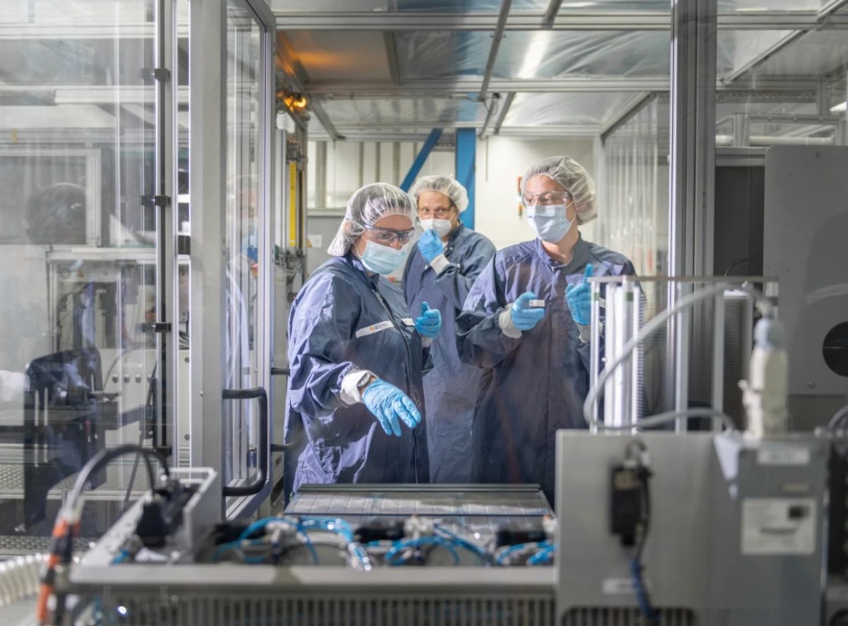
Nexwafe specializes in the development of high-efficiency monocrystalline silicon wafers. The Freiburg, Germany-based company plans to use the funds raised in the Series C financing round to advance the production and commercialization of its epi-wafers.
As part of the investment, Reliance has entered into a strategic partnership with Nexwafe to jointly develop and commercialize Nexwafe's ultra-thin wafers. In return, Reliance will be granted access to the patented technology. The Indian company plans to utilize the technology in its planned gigawatt manufacturing facility in India.
“The commercialization of this promising technology for high-power wafers has strategic importance for Germany, Europe and the world,” said Claas Helmke, partner at Wermuth Asset Management. He added that the efficiency gains provided by the technology are significant. In addition, CO2 emissions from the production of the wafers will be significantly reduced, Helmke said. “These are milestones on the way to the global and sustainable spread of solar technology.”
Kerfless wafer production has been pursued by a number of PV technology developers. Alongside Nexwafe, U.S.-based 1336 Technologies had developed multicrystalline kerfless wafer production – and had achieved promising results in a partnership with Q-Cells. However, the industry switch to monocrystalline technology placed 1366 at a disadvantage, and the company merged with Hunt Perovskite Technologies (HPT) to form a new company, CubicPV, in June of this year.
Alongside allowing for the production of thinner crystalline-silicon wafers, kerfless wafer production also significantly reduces polysilicon production by avoiding the waste material, or kerf, produced through the conventional, diamond wire wafering process.
This content is protected by copyright and may not be reused. If you want to cooperate with us and would like to reuse some of our content, please contact: editors@pv-magazine.com.


3 comments
By submitting this form you agree to pv magazine using your data for the purposes of publishing your comment.
Your personal data will only be disclosed or otherwise transmitted to third parties for the purposes of spam filtering or if this is necessary for technical maintenance of the website. Any other transfer to third parties will not take place unless this is justified on the basis of applicable data protection regulations or if pv magazine is legally obliged to do so.
You may revoke this consent at any time with effect for the future, in which case your personal data will be deleted immediately. Otherwise, your data will be deleted if pv magazine has processed your request or the purpose of data storage is fulfilled.
Further information on data privacy can be found in our Data Protection Policy.