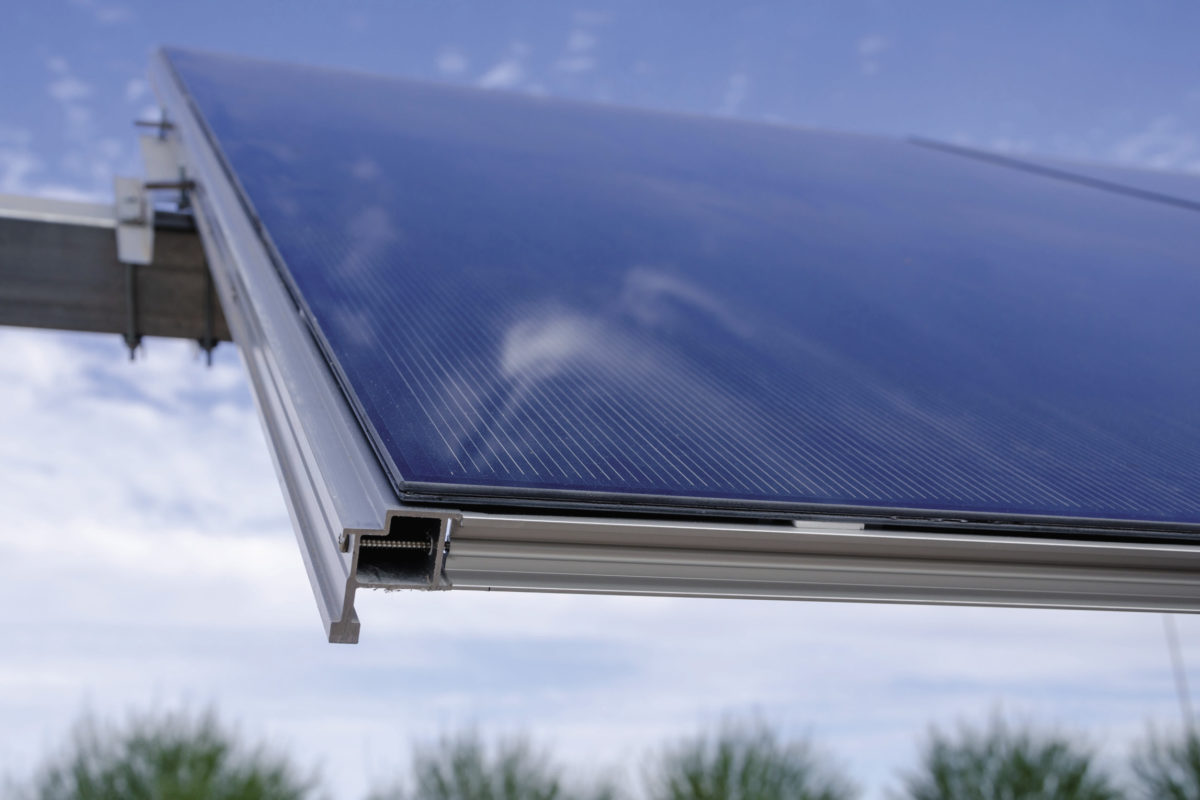
While silicon-based modules still represent more than 90% of the market, cadmium telluride (CdTe) has long represented the largest share of the remainder, able to claim a few advantages over silicon in certain conditions, as well as a lower carbon footprint in manufacturing.
But CdTe is a little way behind silicon in efficiency terms, and still represents only a small share of the market. First Solar set the efficiency record for CdTe at 22.1% back in 2016, and the technology has seen few improvements on the efficiency side since then.
During manufacturing the CdTe material is treated with chlorine, which raises its efficiency typically from less than 5% up into the 20% range. The exact effect of chlorine in this process, and why the process improves efficiency so dramatically, is not fully understood.
Scientists led by Loughborough University in the UK modeled the process, aiming to understand the mechanism involving chlorine. Previous research had noted that defects in the material known as stacking faults disappeared after the chlorine treatment, and this was thought to be linked to the efficiency increase. The work is described in full in the paper Chlorine activated stacking fault removal mechanism in thin film CdTe solar cells: the missing piece, published in Nature Communications.
Grain boundaries
The group showed that the efficiency improvement is actually related to grain boundaries in the crystal, and chlorine’s ability to passivate them – so that electrons no longer become ‘trapped’ in the defects, reducing cell efficiency. “Although the stacking faults disappearance is not what causes the improved efficiency, if they have disappeared then that is the signal that the CdTe cell is going to have good performance,” explained Loughborough researcher Pooja Goddard. “This has never been shown before.”
The group hopes that better understanding the job done by chlorine in CdTe manufacturing will open the door to further efficiencies. Its next plan is to investigate doping with other elements and to continue a project that looks to optimize the interfaces between cell layers. The group is targeting cell efficiencies beyond the 25% mark. “Each small gain in efficiency means the technology is becoming more competitive against the current silicon technology,” commented Goddard.
This content is protected by copyright and may not be reused. If you want to cooperate with us and would like to reuse some of our content, please contact: editors@pv-magazine.com.


By submitting this form you agree to pv magazine using your data for the purposes of publishing your comment.
Your personal data will only be disclosed or otherwise transmitted to third parties for the purposes of spam filtering or if this is necessary for technical maintenance of the website. Any other transfer to third parties will not take place unless this is justified on the basis of applicable data protection regulations or if pv magazine is legally obliged to do so.
You may revoke this consent at any time with effect for the future, in which case your personal data will be deleted immediately. Otherwise, your data will be deleted if pv magazine has processed your request or the purpose of data storage is fulfilled.
Further information on data privacy can be found in our Data Protection Policy.