As today’s silicon solar cells move closer to their theoretical efficiency limit, and the manufacturing industry continues to scale up, even tiny increases in efficiency can add up. And as the industry begins to look to new technologies that promise even higher efficiencies from complex structures, gaining a deeper understanding of the processes at work within the material will always be of value when it comes to improving their performance.
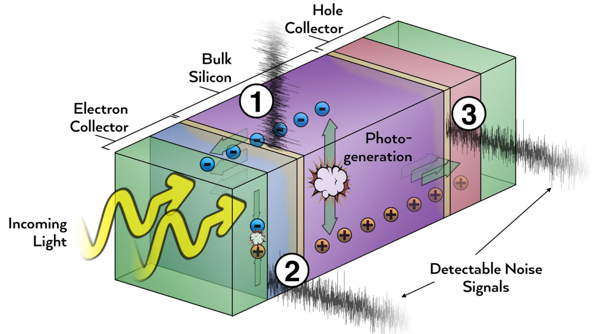
This was on the minds of scientists led by the University of Utah (UU) in the United States, as they sought to measure tiny fluctuations in electrical current as solar cells and pinpoint the sources of electrical noise, accompanying likely efficiency loss, within a silicon solar cell. Many other studies delving into solar cell materials at this level have relied on microscope imaging techniques to observe the processes at work within the cell. However, in this research the group took a different approach, using a technique called cross-correlation noise spectroscopy to pinpoint sources of electrical noise as a charge is generated through the various cell layers.
“Measuring noise on an object is relatively simple. You can just buy devices that do it. But the problem that plagues us is that these devices also have noise,” explained UU associate instructor of physics Kevin Davenport. “This cross-correlation technique allows us to not only measure the noise of the device, but to also measure the noise of our detector and remove it so that we can see much, much smaller noise signals.”
The technique is described in full in the paper Silicon heterojunction solar cells explored via noise spectroscopy: spatial selectivity and the influence of a-Si passivating layers, published in Applied Physics. The group applied its technique to silicon heterojunction cells, and was able to identify several key areas within the cell where noise was generated and further research could lead to better efficiencies.
“We see this wide spectrum of different noise signals and different positions along the frequency axis. We can say, ‘OK, this part of the note that we see, we can attribute to this physical process and this part is a different physical process,’” said Davenport. “But the device is full of these processes that all generate noise and it’s really difficult to un-entangle them—like pulling out a single voice in a 200-person chorus. This technique allows us to remove a lot of the unwanted portion of the signal.”
One key area they identified was the interface between the silicon layer and the transparent electrode, where deposition of the indium-tin-oxide electrode layer somehow modifies the silicon beneath and creates efficiency-reducing defects. A similar noise signal was detected at the interface with the hole transport layer at the rear of the device.
With the ability to monitor the devices and detect sources of noise at this level, the group hopes its work will open up pathways for further research understanding and mitigating their effects on device performance.
This content is protected by copyright and may not be reused. If you want to cooperate with us and would like to reuse some of our content, please contact: editors@pv-magazine.com.


By submitting this form you agree to pv magazine using your data for the purposes of publishing your comment.
Your personal data will only be disclosed or otherwise transmitted to third parties for the purposes of spam filtering or if this is necessary for technical maintenance of the website. Any other transfer to third parties will not take place unless this is justified on the basis of applicable data protection regulations or if pv magazine is legally obliged to do so.
You may revoke this consent at any time with effect for the future, in which case your personal data will be deleted immediately. Otherwise, your data will be deleted if pv magazine has processed your request or the purpose of data storage is fulfilled.
Further information on data privacy can be found in our Data Protection Policy.