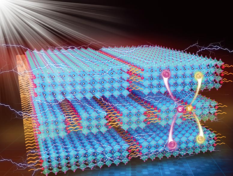
Two-dimensional thin films used in perovskite solar cells that hold promise for commercialisation have been found to have a structure more like two layers of bread with filling in between than the previously assumed “gradient” structure of a cracker with topping.
Findings of new research led by the ARC Centre of Excellence in Exciton Science in collaboration with scientists at Australia’s CSIRO, and Shandong University herald the potential for greater efficiency of perovskite solar cells, and have just been published in the Journal of Materials Chemistry C.
The newly discovered 2D structure — of small-n Ruddlesden Popper perovskites (RPPs) sandwiched between layers of large-n (RPPs) — encourages excitons, the quasiparticles instrumental in converting sunlight to electricity, to move from the central layer to the surfaces of the film. At the same time free carriers transport the resulting charge for collection by electrodes, such that when the perovskite film is incorporated into solar cells they facilitate more efficient solar generation.
“There’s been quite a lot of controversy in the literature” published on the structure of thin-film perovskites, says Professor Ken Ghiggino, one of the authors of the new paper. He adds, “The advance that we’ve achieved is to find out what the real structure of these films is and how they work in a solar cell.”
The ARC researchers based at the University of Melbourne used scanning transmission electron microscopy (STEM), time-resolved photoluminescence and transient absorption measurements to identify the revised understanding of the thin-film materials.
A club sandwich of potential
Two-dimensional perovskite films are a leading contender to form the next generation of solar PV technology and are valued for their stability and durability compared to 3D perovskite cells, their potential low cost, and their likely contribution to the development of light-weight, flexible solar panels. But as recently as February this year, researchers were remarking that they showed “limited charge transport” and a “large bandgap” for solar applications.
“This is the first time a sandwich structure had been proposed versus the conventional gradient distribution model,” says the University of Melbourne’s Dr Fei Zheng, lead author on the new paper. “We think this discovery will help design and device optimisation for higher performance of the 2D cells and LEDs.”
Prototype 2D devices have so far demonstrated 13% efficiency. Researchers can now attempt to drive up that efficiency by changing the thickness of the layers within the ‘sandwich’.
In line with the remit of ARC Centre of Excellence in Exciton Science — which is to discover and develop new materials that improve solar technology, lighting and security systems — 2D perovskite films also have potential application in light-emitting diodes, and photodetectors used in video imaging, security systems, biomedical imaging, gas sensing and optical communications.
This content is protected by copyright and may not be reused. If you want to cooperate with us and would like to reuse some of our content, please contact: editors@pv-magazine.com.


1 comment
By submitting this form you agree to pv magazine using your data for the purposes of publishing your comment.
Your personal data will only be disclosed or otherwise transmitted to third parties for the purposes of spam filtering or if this is necessary for technical maintenance of the website. Any other transfer to third parties will not take place unless this is justified on the basis of applicable data protection regulations or if pv magazine is legally obliged to do so.
You may revoke this consent at any time with effect for the future, in which case your personal data will be deleted immediately. Otherwise, your data will be deleted if pv magazine has processed your request or the purpose of data storage is fulfilled.
Further information on data privacy can be found in our Data Protection Policy.