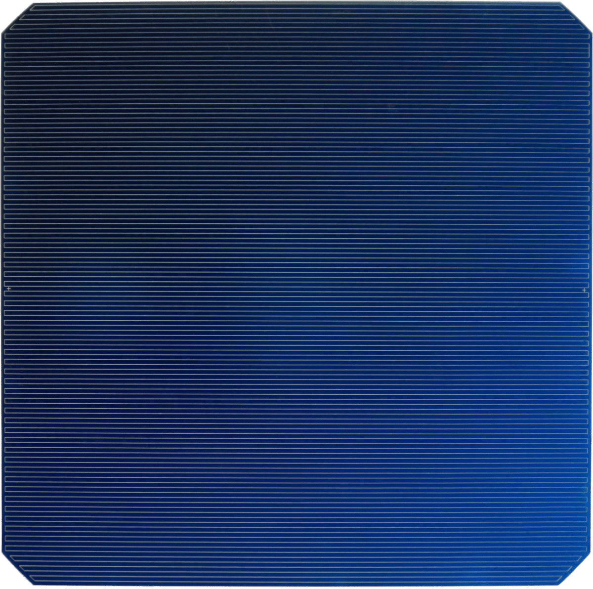
Most tunnel‐oxide passivated contact (TOPCon) solar cells are built with n-type wafers, as their passivating contacts have technical and physical advantages compared to those of p‐type wafers. However, the use of p-type wafers could make it easier to integrate the production of these cells into existing PERC cell lines without having to introduce too many changes into current production processes.
With this in mind, researchers at Germany's Fraunhofer Institute for Solar Energy Systems ISE have sought to improve the production process for high‐efficiency p‐type TOPCon cells. They have identified the best metallization pastes to help reduce contact resistivity and contact recombination by developing a process sequence for the fabrication of such cells.
The scientists started by testing a group of 11 silver (Ag) or silver-aluminum (Ag/Al) metallization pastes. After identifying the most suitable ones, they integrated them into the production process.
“Overall, we observe that for effective contacting, mainly dedicated TOPCon pastes should be used, and some of the pastes which are being promoted for n‐doped TOPCon layers also work quite well for p‐doped TOPCon layers,” the academics explained.
The manufacturing process includes the formation of the p‐type rear contacts through low-pressure chemical vapor deposition (LPCVD) of an in-situ boron-doped polysilicon layer. The process sequence further includes high-temperature annealing and the application of a silicon nitride (SiNx) layer by plasma-enhanced chemical vapor deposition (PECVD) onto both sides of the cell. They said that a 0.2% increase in efficiency via the implementation of a sacrificial SiNx layer for hydrogenation purposes can result in better surface passivation quality of the passivating contact structure.
“Currently, the extra hydrogenation step does indeed add additional cost as another PECVD tool has to be used for depositing the rear silicon nitride (SiNx) layer twice,” researcher Sebastian Mack told pv magazine. “We have not put any effort at all into getting the initial SiNx layer on the rear side high temperature stable, so achieving this would allow for keeping that layer in place and thus lowering cost.”
For the solar cell, the German group used boron‐doped Cz−Si wafers with M2 size.
“We have shown that the best overall results have been achieved for a polysilicon layer thickness of 240 nm,” they said, adding that they achieved a power conversion efficiency of 21.2% under this configuration.
Despite the remarkable efficiency, Mack believes there is much room for improvement.
“Currently, recombination is very much dominated by recombination on the front side and here our process falls somewhat short, and we did not implement a selective emitter here nor apply our best process for front side passivation, which we developed after the experiment,” he said. “In addition, we recently developed a method to reduce the series resistance notably, which by itself should boost efficiency by at least 0.3%.”
Mack said that manufacturer Tempress supplied the polysilicon layers. At the time of the study, there was no way to adapt the polysilicon layer to the requirements of the process sequence.
“And last but not least, the results were from late 2019, but until now, I had no time to write the paper,” he concluded.
The researchers presented their findings in “Progress in p‐type Tunnel Oxide‐Passivated Contact Solar Cells with Screen‐Printed Contacts,” which was recently published in Solar RRL.
This content is protected by copyright and may not be reused. If you want to cooperate with us and would like to reuse some of our content, please contact: editors@pv-magazine.com.


By submitting this form you agree to pv magazine using your data for the purposes of publishing your comment.
Your personal data will only be disclosed or otherwise transmitted to third parties for the purposes of spam filtering or if this is necessary for technical maintenance of the website. Any other transfer to third parties will not take place unless this is justified on the basis of applicable data protection regulations or if pv magazine is legally obliged to do so.
You may revoke this consent at any time with effect for the future, in which case your personal data will be deleted immediately. Otherwise, your data will be deleted if pv magazine has processed your request or the purpose of data storage is fulfilled.
Further information on data privacy can be found in our Data Protection Policy.