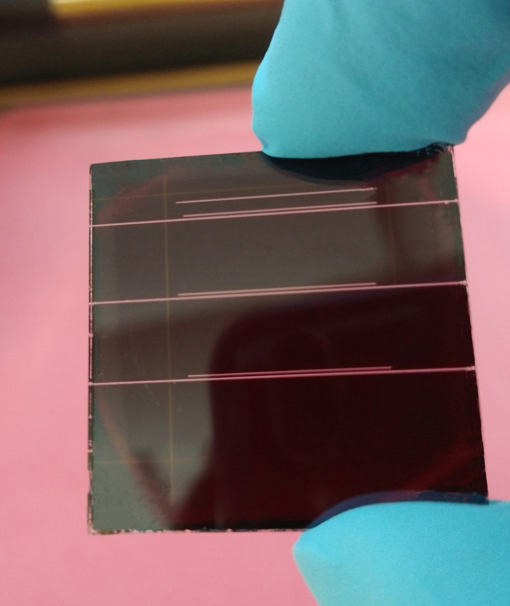
Researchers from HTW Berlin and Helmholtz-Zentrum Berlin (HZB) have investigated the influence of the laser pulse duration for P3 patterning for interconnecting perovskite solar cells, so they can then upscale them into mini photovoltaic modules.
They analyzed the electrical and compositional properties of the scribe lines with the final aim of establishing suitable laser fluence ranges for both nanosecond (ns) and picosecond (ps) lasers, which can ensure robust processes for the fabrication of modules with high average performance.
“The knowledge gained from this study could be directly used in mass production,” researcher Christof Schultz told pv magazine.”This work relies on previous studies that investigated laser-material interaction processes and determined the influence of the laser pulse duration and the laser fluence on the electrical functionality of P2 scribe line.”
The so-called P1, P2, and P3 scribes correspond to the three scribing steps of the process for building the monolithic interconnections that add voltages between cells in modules. The P1 and P3 steps are aimed at isolating the back contact layers of neighboring cells and the P2 step creates an electrical path between the back contact of a cell with the front contact of an adjacent cell.
The P3 step, the academics explained, is often a source of undesired effects such as back contact delamination, flaking, or poor electrical isolation, due to residues that remain in the trench. These issues are likely attributable to interactions between the laser and the material that have not been fully understood to date. According to the scientists, issues with P3 patterning have thus far been reported for both ns and ps patterning.
The German group scribed ns and ps P3 lines on three-cell perovskite solar modules with an area of 2.2 cm2. The P1 and P2 parameters were the same for all the samples. They used surface-analytical techniques, such as scanning electron microscopy (SEM) and energy-dispersive X-ray spectroscopy (EDX), to analyze the morphology and composition of the P3 line. They also used spectrally filtered photoluminescence to map the distribution of the lead iodide (PbI2) within the scribe lines. The patterning of the solar module was performed with a commercial laser system, Rofin Baasel Lasertech.
The scientists achieved the highest power conversion efficiency with ps patterning – around 17% – at a fluence of 2.31 Joule/cm2. With patterning with a significantly more cost-effective ns laser, a higher efficiency of more than 19% was achieved with a fluence of 1.36 Joule/cm2. The scientists said these values are representative of a wide range of suitable fluences for successful P3 patterning.
“Fluences below and above the suitable ranges may lead to lower power conversion efficiencies for both ns and ps pulses,” they said. “Too low fluences would result in incomplete material removal and poor electrical isolations of neighboring cells, while excessively high fluences have a high probability of damaging the front contact layer underneath, due to thermal impact.”
The research team also found that ns patterning results in slightly higher open-circuit voltage and fill factor, which improves module efficiency. The analysis of the materials composition within and aside the scribe line showed that ns patterning results in higher amounts of PbI2 within the lines. Moreover, the ns laser favors the formation of a thin bromine-rich layer at the interface between the perovskite and the hole transport layer (HTL). Both the PbI2 and the bromine-rich layer are able to passivate electronic defect states at the edges of the scribe line and block charge carriers in its vicinity.
‘”Our findings apply to all perovskite compounds based on lead and iodide,” Schultz said.
The scientists described the scribe laser technique in “Improved Electrical Performance of Perovskite Photovoltaic Mini‐Modules through Controlled PbI2 Formation Using Nanosecond Laser Pulses for P3 Patterning,” which was recently published in Energy Technology.
This content is protected by copyright and may not be reused. If you want to cooperate with us and would like to reuse some of our content, please contact: editors@pv-magazine.com.


2 comments
By submitting this form you agree to pv magazine using your data for the purposes of publishing your comment.
Your personal data will only be disclosed or otherwise transmitted to third parties for the purposes of spam filtering or if this is necessary for technical maintenance of the website. Any other transfer to third parties will not take place unless this is justified on the basis of applicable data protection regulations or if pv magazine is legally obliged to do so.
You may revoke this consent at any time with effect for the future, in which case your personal data will be deleted immediately. Otherwise, your data will be deleted if pv magazine has processed your request or the purpose of data storage is fulfilled.
Further information on data privacy can be found in our Data Protection Policy.