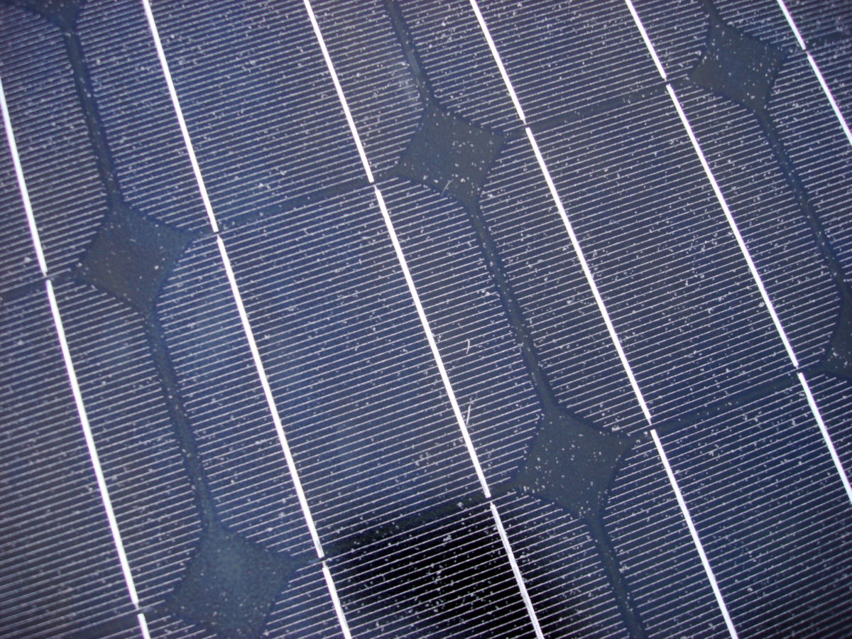
Researchers from Australia’s University of Tasmania and the Australian National University have developed an interdigitated back-contact (IBC) solar cell with an efficiency of 25% and fill factor of 81%.
Their research has been published in Excellent ONO passivation on phosphorus and boron diffusion demonstrating a 25% efficient IBC solar cell, published in Progress in Photovoltaics. The cell is an evolution of a device with 24.4% efficiency developed in earlier studies.
The academics claim to have achieved the 0.6% increase in efficiency through an improvement of the manufacturing process, with a focus on three key factors. They implemented an oxide-nitride-oxide (ONO) passivation stack, optimized diffusion and contact-area fraction, and improved texturing with a monoTEX surfactant. The latter process involved a moderating and wetting agent for alkaline texturing which is known to simplify the texturing of wafers, widen the texturing process window and increase texturing bath lifetime.
The wafers with symmetric ONO stacks were corona charged on the front and rear surfaces with a conventional method. Corona discharge is a technique routinely used to deposit positive or negative charge on the surface of materials. It is commonly adopted in research to characterize the electrical properties of silicon-dielectric interface.
“The ONO stack on phosphorus-diffused wafers was subjected to corona charging at 5.5 kV for 120 seconds, whereas boron-diffused wafers were negatively charged at -6 kV for 100 seconds,” the academics stated. “Notably, the surface passivation is further improved after corona charging.”
The researchers performed the post-oxidation annealing (POA) of the thermal silicon oxide layer immediately after the initial thermal oxidation, to analyze the effect of the surface-doping concentration on the effectiveness of overall ONO passivation quality. The researchers said the operation was conducted in an inert gas ambient which enabled the redistribution of dopants, potentially eliminating abrupt pile-up and depletion at the silicon-silicon oxide (Si/SiO2) interface.
“In summary, the key impact of the observations in this section is that it nullifies the preconception for the need of a POA in inert ambient to achieve good quality passivation for diffused surfaces,” the group said.
The scientists also analyzed the impact of plasma-enhanced chemical vapor deposition (PECVD) for silicon nitride film on the passivation quality of both phosphorus and boron-diffused surfaces. The analysis confirmed additional corona charging is highly beneficial to the surface passivation of both diffused wafers. The Australian team also observed the impact of the thermal silicon oxide thickness on both the optical properties and the surface passivation of various surfaces of the cell.
The academics also used boron-rich-layer (BRL) gettering to improve final bulk lifetime in the IBC cell, with the step applied before ONO passivation growth.
“The average bulk lifetime across six completed cell wafers before metallization was approximately 46ms,” said the researchers. “Such high-bulk life-times were not observed in previous cell fabrication batches.”
Cell performance was measured at Australia’s Scientific and Industrial Research Organization (CSIRO). Testing has already shown the device has an open-circuit voltage of 716 millivolt and a short-circuit current density of 43 milliampere per cm-2.
This content is protected by copyright and may not be reused. If you want to cooperate with us and would like to reuse some of our content, please contact: editors@pv-magazine.com.


Super