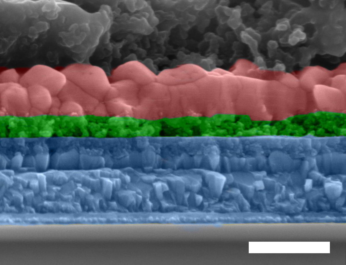
Scientists led by Japan’s Kanazawa University have developed a process for depositing a titanium dioxide electron transport layer (ETL) onto a perovskite. The group claim the method could be scaled up to cut costs for manufacturers moving towards commercial perovskite cell manufacturing.
The ETL plays a key role in carrying electrons from the perovskite into the electrode and separating from ‘holes’ to prevent recombination losses. Titanium dioxide (TiO2) is already commonly used to make the electron transport layer. However, most processes able to deposit a high-quality layer of it onto a perovskite require either high temperatures or a vacuum, which equates to high operating costs.
“Fabricating high-quality, reproducible TiO2 CLs [compact layers] for the efficient performance of planar PSCs [perovskite solar cells] via a scalable, controllable and cost-effective technique remains a significant challenge,” stated the researchers in their paper Oblique electrostatic inject-deposited TiO2 film leads efficient perovskite solar cells, published in Scientific Reports.
Investigating inkjet
To meet the challenge of reducing costs, the group turned to inkjet printing – a process often used in the production of organic PV cells. By developing an optimized process for ETL layer deposition, the researchers were able to produce perovskite solar cells with 13.19% efficiency over an active surface area of 0.09cm².
Positively charged droplets were sprayed onto a negatively charged surface. The group reported previous studies testing similar processes found gravity caused TiO2 to form stacks – resulting in thick, non-uniform layers. However, by simply spraying the precursor at a 45-degree angle to the surface, the group was able to improve uniformity. Varying the coating time allowed the Japanese team to control the thickness of the ETL.
“The ability to control the layer thickness and achieve a uniform, reproducible layer at low cost – without the need for a vacuum – provides a unique package of advantages that has not been reported to date,” said Md Shahiduzzaman, assistant professor at Kanazawa University and the paper’s lead author. “We hope that these properties will lead to effective and commercially relevant scale-up that will contribute to the drive towards cleaner energy worldwide.”
Next steps
The group now plans to investigate how to scale up the process onto larger areas, noting the ‘single nozzle’ approach taken for the paper covers a width of only 5mm, and that ‘cross-talk’ between electric fields around each nozzle could present a challenge to uniform printing with multiple nozzles. The scientists have posited the positioning of a shield around each nozzle as a possible solution.
A further study to coat a variety of substrates in a large scale, high-throughput setting is also planned, and the group has suggested surface engineering or elemental doping of the TiO2 layer could help ensure a good interface between the ETL and the active perovskite, further improving performance.
This content is protected by copyright and may not be reused. If you want to cooperate with us and would like to reuse some of our content, please contact: editors@pv-magazine.com.


1 comment
By submitting this form you agree to pv magazine using your data for the purposes of publishing your comment.
Your personal data will only be disclosed or otherwise transmitted to third parties for the purposes of spam filtering or if this is necessary for technical maintenance of the website. Any other transfer to third parties will not take place unless this is justified on the basis of applicable data protection regulations or if pv magazine is legally obliged to do so.
You may revoke this consent at any time with effect for the future, in which case your personal data will be deleted immediately. Otherwise, your data will be deleted if pv magazine has processed your request or the purpose of data storage is fulfilled.
Further information on data privacy can be found in our Data Protection Policy.