From pv magazine 01/2020
In the first half of 2019, some Tier-1 module makers started promoting the G1 wafer, with vertically integrated company JinkoSolar taking the lead, followed by JA Solar and Trina. Cell makers Tongwei and Aiko Solar both released G1-sized cells and increased the volume of shipments every month.
With wafer sizes going bigger in the second half of 2019, Longi acted first to launch M6 wafers, while Zhonghuan Semiconductor introduced M12 variants to gain a competitive edge. Meanwhile, overseas manufacturers such as LG and Hanwha Q Cells, which adopted the 161.7 mm M4 format earlier to distinguish themselves from their Chinese rivals, are trying to figure out the wafer size for their next-generation products.
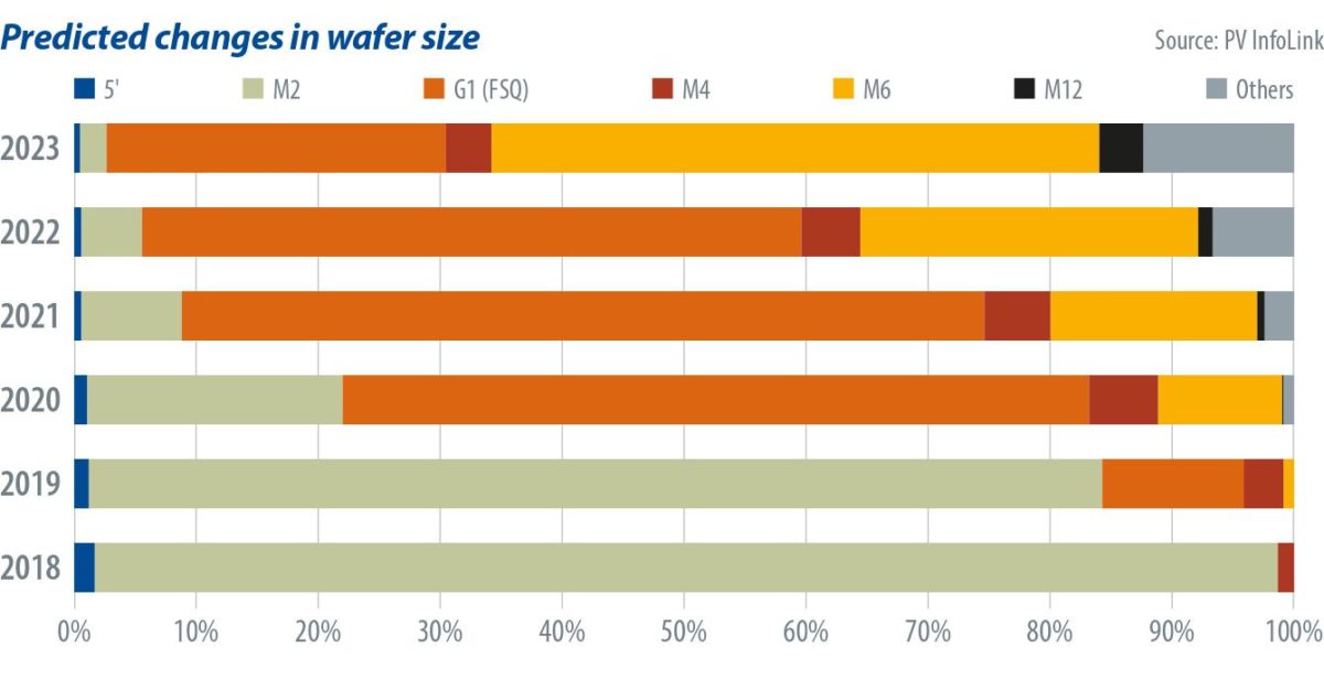
Having said that, most manufacturers have adopted the G1 size for mono-Si wafers and began producing such products in the second half of 2019. However, G1-sized products were predicted to account for a mere 12% of the market in 2019, because it takes time for end users and developers to test and evaluate modules that use larger wafers, and most PV plants that were confirmed in early 2019 will still use M2-sized products.
Technological barriers
Slicing the ingot into M6 size can generate a larger wafer surface area, and hence better price performance compared to G1. Therefore, Longi has actively promoted the M6 wafer and offered prices with a competitive advantage over G1, in the hope of convincing more manufacturers to follow suit. However, apart from Longi and its partner cell suppliers, other mono-Si manufacturers remain uncertain about switching to M6. At present, these manufacturers are only accommodating new lines with M6 wafers and are producing only once orders are placed.
Behind this conservative attitude are high implementation barriers, which require large cell and module equipment modification, as well as high capex requirements – more than two to three times the price required to adopt G1. On the other side, both Canadian Solar and GCLSI have adopted the M6 size for their multi-Si and cast-mono wafers.
There are technological barriers associated with the application of the M6 and M12 formats, especially with the manufacturing process for wafers and cells. For wafer makers, the breakage rate of larger wafers is higher during the thinning process. In terms of the cell manufacturing process, uneven surfaces might occur during the texturing and coating process, and result in a slight decrease in cell efficiency.

Accelerated withdrawal
After adopting larger wafer and module techniques, mono PERC modules are increasingly edging out multi-Si products for their ability to deliver competitive performance. Consequently, demand for multi-Si products weakened significantly in October 2019, with multi-Si cell prices falling sharply to a new low, hitting $0.079/W in mid-December. While sending ripples across the wafer and polysilicon segments, weak cell prices also caused prices of multi-Si modules to fall. Despite the low prices, demand for multi-Si products will probably not recover this year due to the widened gap that results from significant improvements in wattage output and price reductions for mono-Si products. Taking 72-cell module as an example, the mainstream wattage output of mono modules will hit 390-400 W, whereas that of multi modules might hover around 340-350 W, even when using larger wafers and half-cut techniques. With 50 W of the wattage gap and a price difference of only $0.03-0.04/W, multi modules are no longer appealing to end users.
Cast mono, which entered commercial production in 2019, is facing more pressure from mono-Si wafers, which have achieved further price reductions this year. Against this backdrop, the development of cast mono will depend on the difference between polysilicon prices for mono- and multi-Si wafers this year.
In terms of size format, it’s difficult for older multi-Si wafer and cell production lines to upgrade to M6. Moreover, demand for multi-Si product continues to weaken, while multi-Si cells are no longer profitable. Thus, manufacturers are unwilling to upgrade existing lines or expand capacity. In fact, these producers have started converting lines from multi-Si to mono-Si, and those with older production lines may withdraw from the market. It’s expected that the share of multi-Si products will decrease to less than 20% this year.
Market prospects
Wafer size standardization is necessary for manufacturers to achieve economies of scale. A monopoly market with only a few larger wafer suppliers would be an unfavorable outcome for the downstream sector.
PV InfoLink projects that four different wafer sizes will remain in the market this year. G1 mono wafers will remain mainstream, accounting for 58% of the market, while M6 wafers will steadily gain ground to an approximate share of 9%.
The views and opinions expressed in this article are the author’s own, and do not necessarily reflect those held by pv magazine.
This content is protected by copyright and may not be reused. If you want to cooperate with us and would like to reuse some of our content, please contact: editors@pv-magazine.com.


2 comments
By submitting this form you agree to pv magazine using your data for the purposes of publishing your comment.
Your personal data will only be disclosed or otherwise transmitted to third parties for the purposes of spam filtering or if this is necessary for technical maintenance of the website. Any other transfer to third parties will not take place unless this is justified on the basis of applicable data protection regulations or if pv magazine is legally obliged to do so.
You may revoke this consent at any time with effect for the future, in which case your personal data will be deleted immediately. Otherwise, your data will be deleted if pv magazine has processed your request or the purpose of data storage is fulfilled.
Further information on data privacy can be found in our Data Protection Policy.