From pv magazine, July edition
Every year, PV manufacturers, material suppliers and equipment providers use the SNEC show in Shanghai to unveil their new products and plans. Unlike last year, when many companies announced capacity expansion plans, 2019 saw manufacturers stressing their R&D efforts and tech innovations, several of which are worth highlighting.
Module output exceeding 400 W
Last year, only a few manufacturers displayed 72-cell, 400 W+ modules. But this year, such higher-output modules were a common sight at SNEC, with several manufacturers trying to achieve output levels above 400 W. In particular, this year more manufacturers showcased n-type modules at the SNEC show. Companies such as JinkoSolar, Jolywood, and Trina Solar all displayed TOPCon modules, while Jinergy, GS Solar, Tongwei, Risen and CIE Power exhibited heterojunction (HJT) modules. Among them, GS Solar’s second-generation HDT modules integrate HJT and interdigitated back contact (IBC) technologies. In addition, SunPower unveiled its brand new 6-inch cell IBC modules.
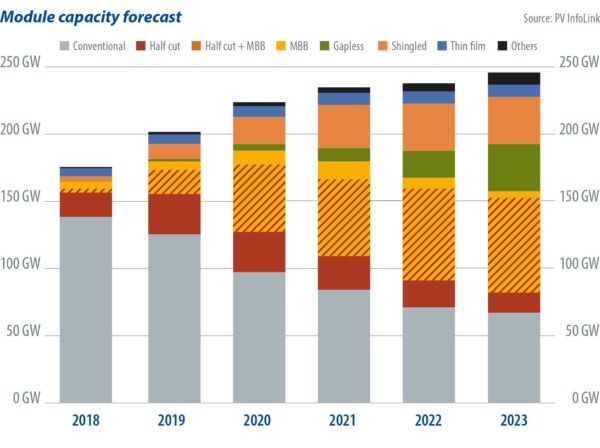
Given that module surface area isn’t going to become indefinitely bigger, assembling more PV cells or reducing spacing between them is another way to enhance output. In addition to shingled technology, which has become more common over the past two years, 2019 saw the emergence of similar technologies such as paving, narrowed spacing, overlap and superposition welding — all of which PV InfoLink categorizes as “high-density” modules.
Superposition welding and overlap techniques increase gain in light absorption by arranging cut-cells in an overlapping manner. Unlike shingled modules, which connect cells with conductive paste, these techniques involve highly elastic ribbon. Superposition welding and overlap also requires less effort to accommodate these two technologies in production than shingled ones. This year, Jinko, Trina and HaiTai Solar showcased gapless modules.
Paved modules, which were already exhibited at PV Expo Japan earlier this year, are different from superposition welding and overlap. Instead of overlaying solar cells, paved modules use elastic and triangular ribbons to connect half-cut cells tightly, to reduce spacing and add more cells to the modules, without losing light-absorbing surface area.
“Added-cell” and larger wafers
In addition to high-efficiency cell or module technologies, many manufacturers achieve higher output by assembling more cells, known as “added-cell” modules, or by increasing wafer size. Earlier this year, some companies mass-produced 78-cell modules up to 400 W by adopting the half-cut technique. However, as the real efficiency of added-cell modules is not increased significantly, 60-cell and 72-cell modules will remain mainstream.
For mono-Si wafers, 158.75mm full square will become the most adopted design by the second half of the year. Only a few manufacturers use wafers that are larger than this. LG and Hanwha Q Cells, for instance, use M4 wafers (161.7mm), while Longi is promoting 166mm wafers.
For p-type modules to exceed 400 W, it’s more feasible to adopt module technologies, assemble more cells or use larger wafers. High-density modules offer better efficiency than half-cut, multi-busbar, or added-cell designs. Superposition welding and narrowed spacing approaches have gained much attention from module makers, as they only need to adjust existing equipment to accommodate the two.
Whether the new technologies will grab market share depends on the maturity of materials and technologies, as well as the development of equipment suppliers. If development goes smoothly, it is likely that companies will see some cannibalization of the market for shingled modules. That will also make module companies re-evaluate their technology roadmaps for high-density modules.
Cast mono back in the spotlight
The cast-mono method has become far more mature than it was just eight years ago, with improvements in efficiency and appearance. Also, the transition to larger wafers make cast mono stand out for its competitiveness in cost and yield rate. However, cast mono still has to overcome issues such as dislocation density, appearance and price-performance ratio. Despite being slightly cheaper than mono-Si, some believe that customers will not favor cast-mono products because they have lower efficiencies. If these issues can be resolved, cast-mono products might be able to grab market share.
During SNEC, GCL — the cast-mono giant — announced a 6 GW deal to cooperate with Canadian Solar, Astronegy, Sunport Power and Akcome. The group also unveiled a plan to complete upgrades to 1,400 casting furnaces in 2020. Larger-scale production of cast mono is therefore expected after the third quarter.
Recently, the module sector saw an increase in order volumes for cast-mono products. Though some cell and module makers remain conservative about cast mono, most companies are planning to develop such products. PV InfoLink believes that manufacturers of multi-Si wafers and multi-Si cells will pivot to cast mono. However, these manufacturers’ moves will depend on the development of leading companies, as well as order volumes, from the second half of next year.
Module technology is innovating at a faster pace this year. On the mono-Si product side, the market will see wafer sizes shift to 158.75mm and its adoption of half-cut and MBB between the second half of this year and 2020. As this requires big equipment adjustments, 166mm wafers will not become mainstream in the near term. Only Canadian Solar’s multi-Si, as well as Longi and its business partners, will develop them over the short term. In terms of multi-Si products, progress is slower in terms of wafer size.
From the perspective of market demand, as there won’t be an immediate installation boom in the Chinese market in July, Q3 demand might be slightly lower than anticipated. Looking at the market situation so far, demand is steady from Q1 to Q3, but there will be a significant rebound in Q4, as expected.
The current demand forecast projects that the supply chain for mono-Si products will see shortages of polysilicon and wafers. As a result, it is expected that prices for polysilicon for mono-Si and mono-Si wafers will steadily rise in the third quarter, whereas cell and module prices will remain stable. Prices for multi-Si products, on the other hand, will be flat in the third quarter due to a polysilicon surplus. Nevertheless, the revival of Chinese demand will drive up prices for multi-Si wafers, cells and modules in Q3.
As module output remains high and might even go up, materials such as EVA and glass have witnessed strong price jumps. Given that PERC cell prices remain high, as well as the upward trend in multi-Si cell prices, manufacturers that only produce modules will record lower profitability, despite higher demand for panels this year. In fact, the module sector has become the industry in which it is the most difficult to make profits along the supply chain.

The views and opinions expressed in this article are the author’s own, and do not necessarily reflect those held by pv magazine.
This content is protected by copyright and may not be reused. If you want to cooperate with us and would like to reuse some of our content, please contact: editors@pv-magazine.com.


By submitting this form you agree to pv magazine using your data for the purposes of publishing your comment.
Your personal data will only be disclosed or otherwise transmitted to third parties for the purposes of spam filtering or if this is necessary for technical maintenance of the website. Any other transfer to third parties will not take place unless this is justified on the basis of applicable data protection regulations or if pv magazine is legally obliged to do so.
You may revoke this consent at any time with effect for the future, in which case your personal data will be deleted immediately. Otherwise, your data will be deleted if pv magazine has processed your request or the purpose of data storage is fulfilled.
Further information on data privacy can be found in our Data Protection Policy.